
Heat dissipation bump electrode for chip on film

a bump electrode and chip technology, applied in the field of semiconductor packaging, can solve the problems of high cost of cof package, inefficient heat dissipation of functional elements generating high heat, and insufficient heat dissipation

Active Publication Date: 2018-11-06
LAPIS SEMICON CO LTD
View PDF16 Cites 0 Cited by
  • Summary
  • Abstract
  • Description
  • Claims
  • Application Information

AI Technical Summary

Benefits of technology

The present invention provides a semiconductor package that effectively dissipates heat without increasing its size. This is achieved by placing a second bump electrode for heat-dissipation around the high temperature area of the semiconductor chip and forming a heat relay line on the wiring substrate where the semiconductor chip is mounted. This results in a heat dissipation route specifically for the high temperature area, allowing for efficient heat dissipation without the need for an increase in the size of the semiconductor package.

Problems solved by technology

Here, there may be a functional element consuming a large amount of current resulting in generating heat much more than other functional elements among plural functional elements formed on the semiconductor chip.
Therefore, depending on the position of the functional element generating the high heat within the semiconductor chip, the heat dissipation may not be achieved efficiently from the functional element generating the high heat.
However there occurs a problem incurring high cost of the COF package since enlargement of the COF package is needed to take such heat dissipation countermeasures.

Method used


Image

  • Heat dissipation bump electrode for chip on film
  • Heat dissipation bump electrode for chip on film
  • Heat dissipation bump electrode for chip on film

Examples


Embodiment Construction

[0023]Embodiments of the present invention will now be described in detail with reference to the accompanying drawings.

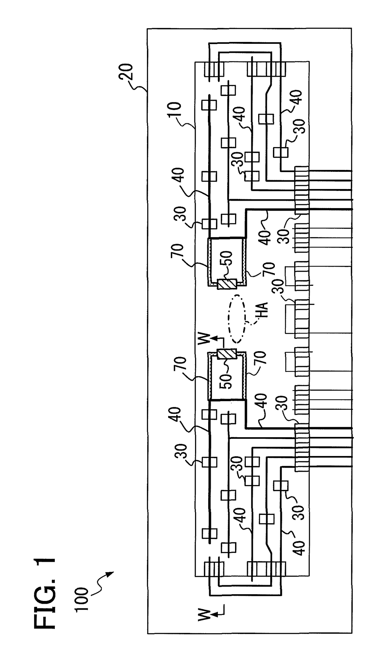
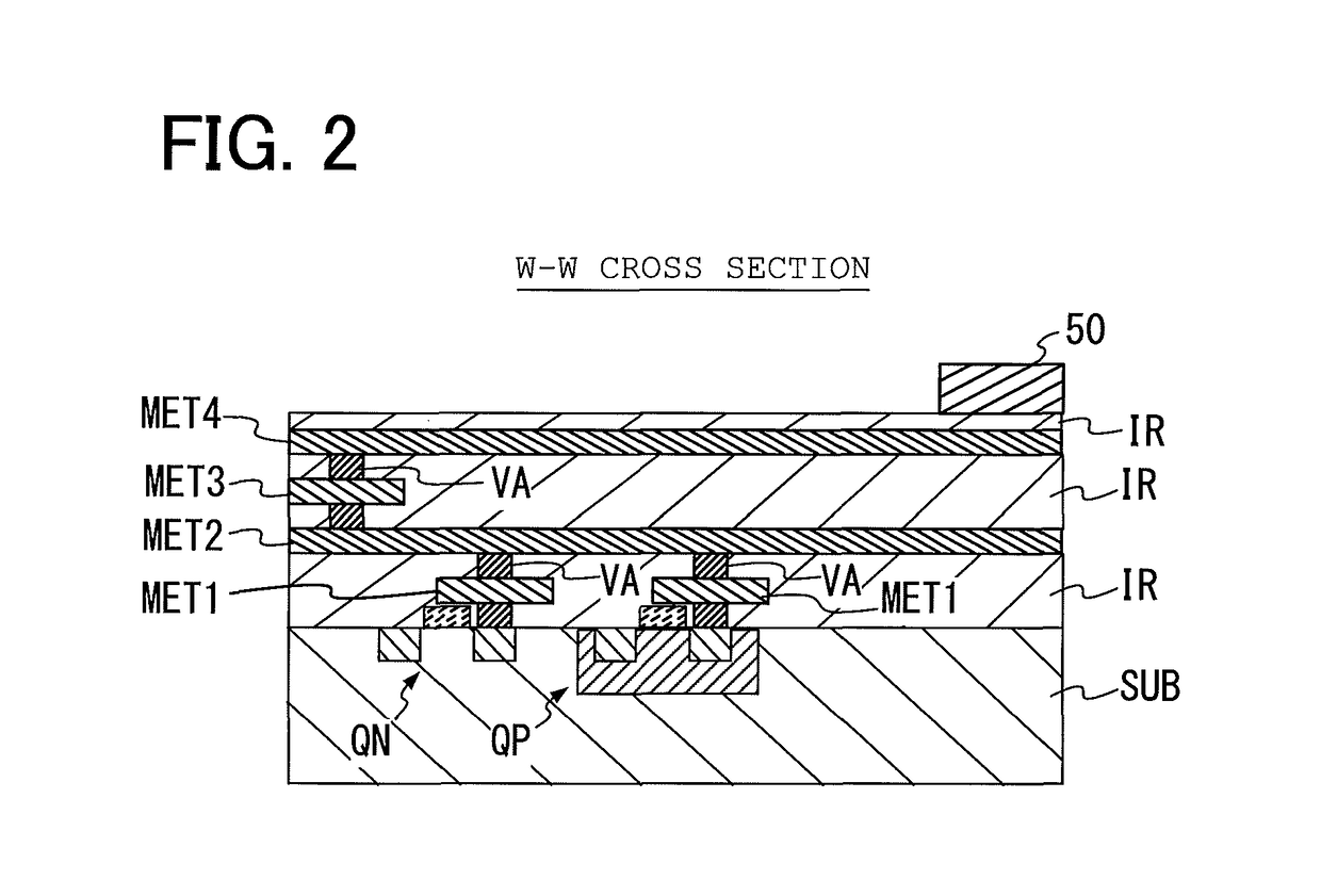
[0024]FIG. 1 is a transparent diagram showing a COF package 100 as a semiconductor package according to the present invention when the COF package is viewed from just above it.

[0025]The COF package 100 includes a semiconductor IC (Integrated Circuit) chip 10 and a filmy flexible wiring substrate 20 made of polyimide resin or the like. The semiconductor IC chip 10 is mounted on the flexible wiring substrate 20. Besides, in FIG. 1, a surface of the semiconductor IC chip 10 and a surface of the flexible wiring substrate 20 are overlapped and shown wherein the both surfaces is a bonded face when the semiconductor IC chip 10 is mounted on the flexible wiring substrate 20.

[0026]The semiconductor IC chip 10 has an LCD driving circuit for driving an LCD panel formed therein, for example. There are a plurality of bump electrodes 30 as first bump electrodes formed on the surf...


PUM

PropertyMeasurementUnit
temperatureaaaaaaaaaa
source voltageaaaaaaaaaa
metallicaaaaaaaaaa

Abstract

A dummy bump electrode for heat-dissipating is provided on a surface of a semiconductor chip. The semiconductor chip is mounted on a wiring substrate. A lead line is formed on the wiring substrate. The heat-dissipating bump electrode and a lead line are connected to each other through a heat dissipation pattern, thereby efficiency of the heat dissipation is improved.

Description

BACKGROUND OF THE INVENTION[0001]Field of the Invention[0002]The present invention relates to a semiconductor package comprising a semiconductor chip and a wiring substrate.[0003]Description of the Related Art[0004]Currently a COF (Chip On Film) package is known as a semiconductor package in which, e.g. a semiconductor chip having a circuit for driving a Liquid Crystal Display panel is formed on a wired circuit substrate of film made of polyimide or the like (See Japanese Patent Application Kokai No. 2008-270453, for example). This circuit is called an LCD driving circuit hereinafter.[0005]Further, in recent years, it is desired to supply an LCD driving circuit operable with high-speed and high-capacity in order to comply with upsizing of the LCD panel and heightening precision of the LCD panel. This trend causes the heat up of the semiconductor chip of the LCD driving circuit.SUMMARY OF THE INVENTION[0006]The heat generated by the semiconductor chip is dissipated from a bump electr...

Claims


Application Information

Patent Timeline
Patent Type & Authority Patents(United States)
IPC IPC(8): H01L23/34G09G3/36H01L23/367H05K7/16H01L21/00G02F1/1333H01L23/522H01L23/00
CPCH01L23/3677G02F1/1333G09G3/3648G09G3/3696H01L24/14H01L2224/16235H01L24/16H01L2224/14152H01L2224/14519H01L2224/16227H01L23/522G09G3/3685G09G2300/0426
Inventor ICHIKURA, HIROYOSHI
Owner LAPIS SEMICON CO LTD
Learn More