Silicon-based component with at least one chamfer and its fabrication method

a technology of micro-mechanical components and chamfers, which is applied in the field of silicon-based micro-mechanical components with at least one chamfer, can solve the problems of unsatisfactory vertical etches b>5/b>, and achieve the effect of improving the mechanical strength of components and improving aesthetics

Active Publication Date: 2019-02-05
NIVAROX FAR
View PDF13 Cites 3 Cited by
  • Summary
  • Abstract
  • Description
  • Claims
  • Application Information

AI Technical Summary

Benefits of technology

[0008]It is an object of the present invention to overcome all or part of the aforecited drawbacks by proposing a new type of silicon-based micromechanical component and a new type of fabrication method, in particular, to improve the aesthetics and to improve the mechanical strength of components formed by micromachining a silicon-based wafer.
[0015]It is understood that two distinct types of etch are obtained in the same etching chamber without removing the substrate from the chamber. It is immediately clear that the oblique etching in step c) removes the substantially right-angled edges respectively between the vertical peripheral or inner walls etched to form several micromechanical components in the same substrate and the upper and lower surfaces of the substrate. It can also be observed that the oblique etching in step c) allows for a considerably more open angle and a substantially rectilinear direction of etching, which avoids being limited by the parameters of a “Bosch” deep reactive ion etching, which is, conversely used in step d) with optimised vertical etching parameters.
[0022]in step g), the continuous etching and passivation gas flows are pulsed to enhance the etching at the bottom level;
[0026]Advantageously according to the invention, the micromechanical component enjoys a considerable aesthetic improvement by forming components which have a much more elaborate aesthetic finish. Further, the substantially rectilinear chamfered surface provides improved mechanical strength, particularly by reducing the possibility of chips to the substantially right-angled edges respectively between the vertical peripheral and / or inner walls and the upper and / or lower surfaces of the micromechanical component.
[0027]It is also clear that the vertical peripheral and / or inner walls provide a reduced contact surface offering an improvement as regards tribological contact with other components or as regards the insertion of a member along an inner wall of the micromechanical component. Finally, the recessed areas of the vertical peripheral and / or inner walls are more open as a result of the chamfered surface which may enable an increase in volume capacity for receiving adhesive or lubricant.

Problems solved by technology

After several years of fabrication, it was found that these vertical etches 5 were not entirely satisfactory, particularly due to the right-angled edges which are prone to chipping and to the “crude” nature of the components obtained.

Method used


Image

  • Silicon-based component with at least one chamfer and its fabrication method
  • Silicon-based component with at least one chamfer and its fabrication method
  • Silicon-based component with at least one chamfer and its fabrication method

Examples


first embodiment

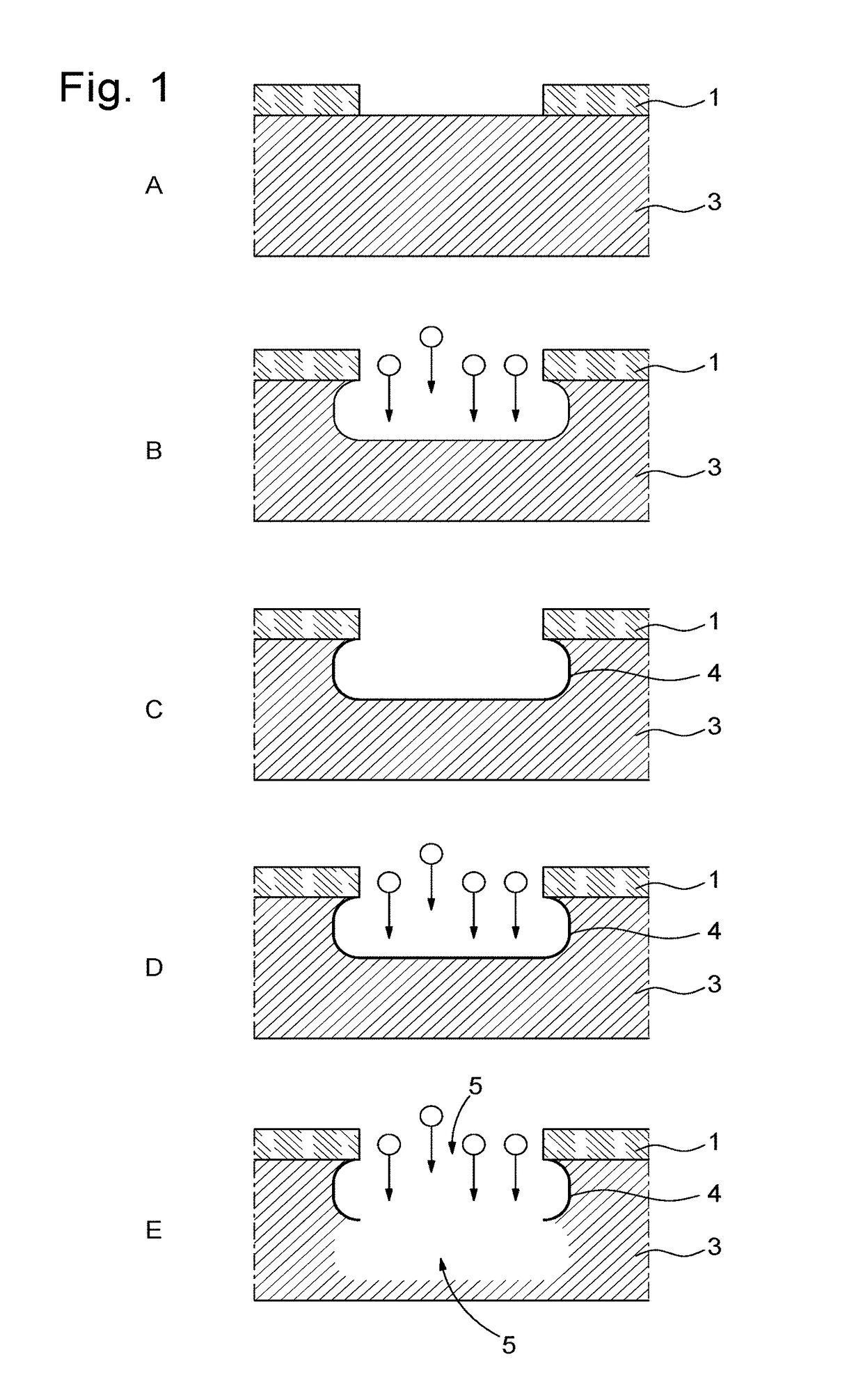
[0039]The invention relates to a method 11 for fabricating a silicon-based micromechanical part. As illustrated in FIG. 18, method 11 illustrated in a single line, includes a first step 13 consisting of taking a silicon-based substrate.

[0040]The term “silicon-based” means a material including single crystal silicon, doped single crystal silicon, polycrystalline silicon, doped polycrystalline silicon, porous silicon, silicon oxide, quartz, silica, silicon nitride or silicon carbide. Of course, when the silicon-based material is in crystalline phase, any crystalline orientation may be used.

[0041]Typically, as illustrated in FIG. 9, the silicon-based substrate 41 may be a silicon-on-insulator substrate (also known by the abbreviation “SOI”) comprising an upper silicon layer 40 and a lower silicon layer 44 joined by an intermediate silicon oxide layer 42. However, alternatively, the substrate could comprise a silicon layer added to another type of base such as, for example, a metal bas...

second embodiment

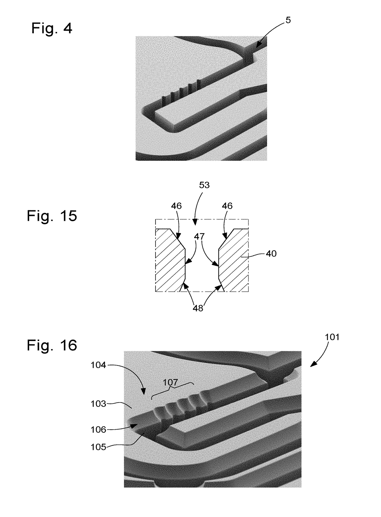
[0061]Thus, after step 19 of forming etch 51, method 11 of the second embodiment continues with step 25 of forming a protective layer 52 on oblique walls 46 and substantially vertical walls 47, leaving the bottom of etch 51 without any protective layer, as seen in FIG. 12.

[0062]Preferably, protective layer 52 is formed of silicon oxide. Indeed, as seen in FIGS. 11 and 12, step 25 may then comprise a first phase 24 intended to oxidise the entire top of substrate 41, i.e. mask 43 (when made of silicon oxide), and the walls of etch 51, to form an added thickness on mask 43 and a thickness on oblique walls 46, vertical walls 47 and the bottom of etch 51, to form the protective silicon oxide layer 52, as seen in FIG. 11.

[0063]The second phase 26 could then consist in directionally etching protective layer 52 in order to selectively remove the horizontal silicon oxide surfaces from a part of mask 43 and from the entire part of protective layer 52 only on the bottom of etch 51 as seen in F...

third embodiment

[0080]Thus, after phase 22 of deoxidizing substrate 41, method 11 continues with step 29 of filling a cavity created during etchings 17, 19 and 27 of the micromechanical component, formed by an upper chamfered surface, a peripheral wall and a lower chamfered surface, with a metal or metal alloy in order to provide an attachment to the micromechanical component.

[0081]In a preferred example, lower layer 44 of substrate 41 is highly doped and used as the direct or indirect base for filling by electroplating. Thus, step 29 could include a first phase 30 of forming a mould, for example made of photosensitive resin, on top of mask 43 and in a part of etch 53. A second phase 32 could consist in electroplating a metal part 112, from lower layer 44, at least between the micromechanical silicon-based component and a part of the mould formed in etch 53. Finally, a third phase 34 could consist in removing the mould formed in the phase 30.

[0082]The third embodiment ends with phase 23 of releasi...


PUM

PropertyMeasurementUnit
angleaaaaaaaaaa
angleaaaaaaaaaa
angleaaaaaaaaaa

Abstract

The invention relates to a silicon-based component with at least one chamfer formed from a method combining at least one oblique side wall etching step with a “Bosch” etching of vertical side walls, thereby enabling aesthetic improvement and improvement in the mechanical strength of components formed by micromachining a silicon-based wafer.

Description

[0001]This application claims priority from European Patent Application No. 15173823.4 filed on Jun. 25, 2015, the entire disclosure of which is hereby incorporated by reference.FIELD OF THE INVENTION[0002]The invention relates to silicon-based micromechanical component with at least one chamfer and a method for fabrication of the same. More specifically, the invention relates to such a component formed by micromachining a silicon-based wafer.BACKGROUND OF THE INVENTION[0003]CH Patent 698837 discloses the fabrication of a timepiece component by micromachining a wafer of amorphous or crystalline material, such as crystalline or polycrystalline silicon.[0004]Such micromachining is generally obtained by deep reactive ion etching (also known by the abbreviation “DRIE”). As illustrated in FIGS. 1 to 4, a known micromachining method consists in structuring a mask 1 on a substrate 3 (cf. FIG. 1, step A) followed by a “Bosch” deep reactive ion etching combining in succession an etching phas...

Claims


Application Information

Patent Timeline
Patent Type & Authority Patents(United States)
IPC IPC(8): B44C1/22C23F1/00G04D99/00B81C1/00H01L21/3065H01L21/32
CPCG04D99/00B81C1/00103C23F1/00B81C2201/0138B81B2203/0384B81C2201/014B81C2201/0132B81B2201/035B81B1/00B81C1/00531G04B17/066G04B37/22G04B19/12B81C1/00087B81C99/008
Inventor GANDELHMAN, ALEX
Owner NIVAROX FAR
Why Eureka
Try Eureka