
Method for application of an overgrowth layer on a germ layer

Active Publication Date: 2019-03-26
EV GRP E THALLNER GMBH
View PDF8 Cites 0 Cited by
  • Summary
  • Abstract
  • Description
  • Claims
  • Application Information

AI Technical Summary

Benefits of technology

The patent text describes a method for efficiently producing semiconductor components by using imprint technologies. This method saves time and reduces the steps required to create the components. The imprinted structures can be left in the epitaxial layer without negatively impacting their properties. The method also reduces the formation of a residual layer by displacing mask material and eliminates the need for subsequent etching steps. The mask material can be thermally hardened, with temperatures reaching more than 750°C. The method also allows for the demolding of the imprint stamp without destroying the imprinted structures, and the growth of the overgrowth layer can be detected through a decrease in fault density.

Problems solved by technology

In very many cases, it is not possible to use simple polymer-based photoresists, as the masks must be comprised of a hard material layer.
Material deposition and above all the etching processes consequently become more difficult, more complicated and more expensive.

Method used


Image

  • Method for application of an overgrowth layer on a germ layer
  • Method for application of an overgrowth layer on a germ layer
  • Method for application of an overgrowth layer on a germ layer

Examples


Embodiment Construction

[0214]In the figures, the same components or components with the same function are labelled with the same reference numbers.

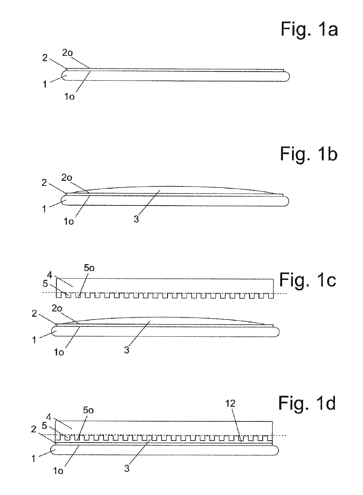
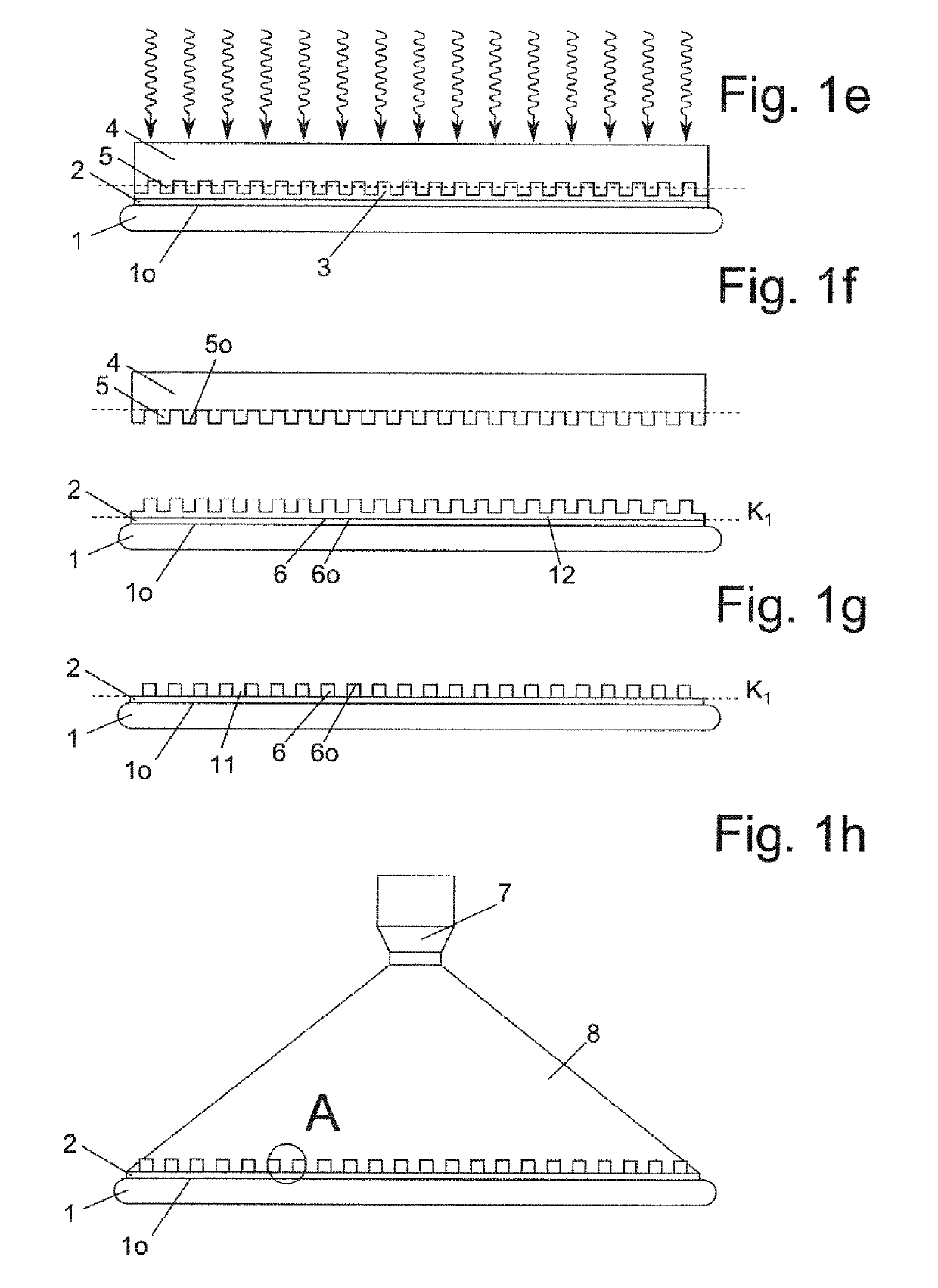
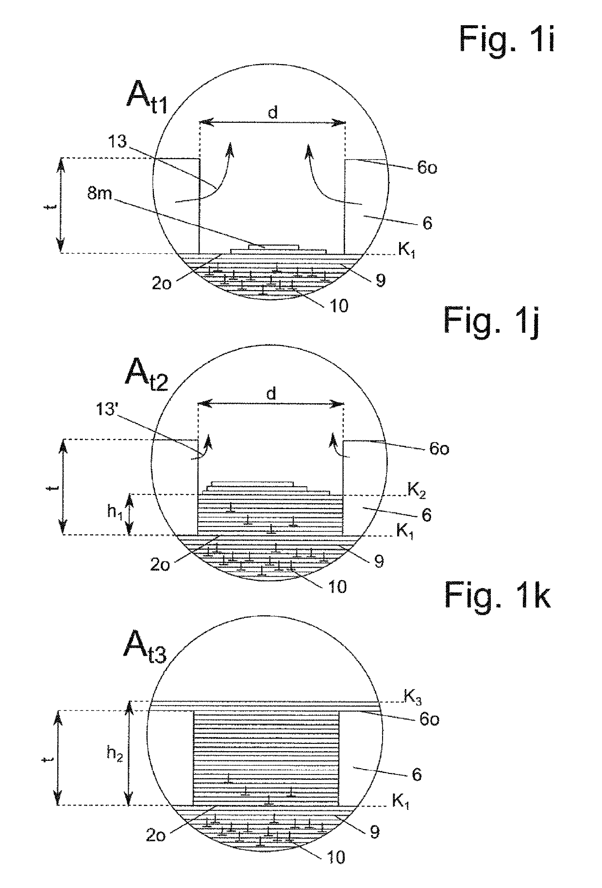
[0215]All of the figures shown exclusively constitute schematic illustrations, which are not true to scale, of conceivable process steps according to the invention. In particular, the order of magnitude of the structures of a mask 6 for masking a seed layer 2 lie in the micro- and / or nanometre range. An overgrowth layer 14 is applied onto the mask 6 and the seed layer 2.

[0216]FIG. 1a shows a cross-sectional illustration of a substrate 1 with a substrate surface 1o, on which the seed layer 2 is or has been deposited in a first process step with a seed layer surface 2o. According to an alternative embodiment, the substrate 1 itself can be the seed layer 2. The seed layer 2 is preferably monocrystalline, more preferably monocrystalline and epitaxial. It is possible in particular to influence the crystal orientation of the seed layer 2 by means of the deposition me...


PUM


Abstract

A method for applying a masked overgrowth layer onto a seed layer for producing semiconductor components, characterized in that a mask for masking the overgrowth layer is imprinted onto the seed layer.

Description

FIELD OF THE INVENTION[0001]The invention relates to a method for applying an overgrowth layer onto a seed layer for producing semiconductor componentsBACKGROUND OF THE INVENTION[0002]In the semiconductor industry, the creation of high-purity, but above all also defect-free layers is of great importance for the production of semiconductor components. Defects, particularly crystal defects, have a decisive influence on the functionality and durability of semiconductor components. Very many semiconductor components are manufactured directly on monocrystalline substrates, which have an extremely high purity and relatively low defect density. Semiconductor substrates of such a type are produced using special processes, particularly the Czochralski process. For the most part, methods of this type create a very large single crystal, which is sawn or cut in further process steps to give the individual substrates.[0003]Very often it is necessary to create further monocrystalline layers with ...

Claims


Application Information

Patent Timeline
IPC IPC(8): B32B3/02C30B23/04C30B25/04H01L21/02G03F7/00
CPCG03F7/0002C30B23/04C30B25/04H01L21/0242H01L21/02647H01L21/02433H01L21/02439H01L21/02521H01L21/02642H01L21/02381
Inventor KREINDL, GERALDZAGLMAYR, HARALDEIBELHUBER, MARTIN
Owner EV GRP E THALLNER GMBH
Learn More