Semiconductor device

a technology of semiconductors and devices, applied in the field of semiconductor devices, can solve the problems of laser output decline, performance degradation of semiconductor laser elements, etc., and achieve the effect of ensuring stability

Active Publication Date: 2019-05-14
PANASONIC INTELLECTUAL PROPERTY MANAGEMENT CO LTD
View PDF24 Cites 0 Cited by
  • Summary
  • Abstract
  • Description
  • Claims
  • Application Information

AI Technical Summary

Benefits of technology

[0007]Conventional semiconductor laser device 900 is configured such that filler 907 made of an Ag paste or a solder material is filled between LD bar 903 and lead-out electrode 906 to improve the thermal conductivity. However, when an Ag paste or a solder material is filled between LD bar 903 and lead-out electrode 906, the difference in the coefficient of thermal expansion between LD bar 903 and lead-out electrode 906 may cause a crack at the interface between lead-out electrode 906 and filler 907 or inside filler 907. The development of such crack causes a decrease in thermal conductivity and a decrease in electrical connection (in other words, an increase in electrical resistance) between LD bar 903 and lead-out electrode 906, thereby causing performance degradation or breakdown of the semiconductor laser device.
[0009]As described above, according to the present disclosure, the provision of the metal layer and the metal sheet between the bump and the second electrode block allows a stress caused by the difference in the coefficient of thermal expansion between the semiconductor element and the second electrode block to be relaxed, and allows an electrical connection between the semiconductor element and the second electrode block to be stably ensured.

Problems solved by technology

When reaching a high temperature, semiconductor laser elements suffer performance degradation, such as a decrease in laser output.

Method used


Image

  • Semiconductor device
  • Semiconductor device
  • Semiconductor device

Examples


first exemplary embodiment

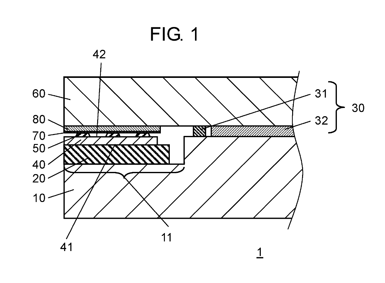
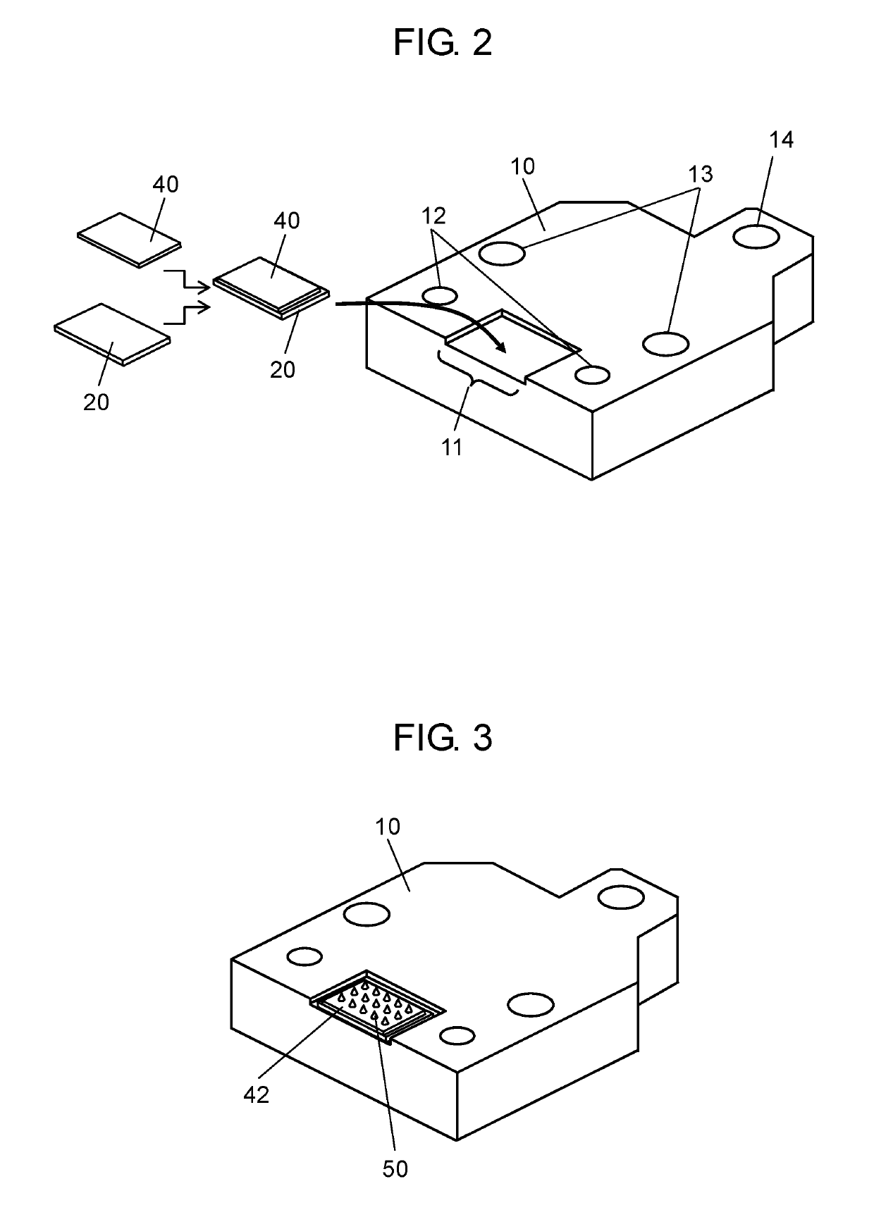
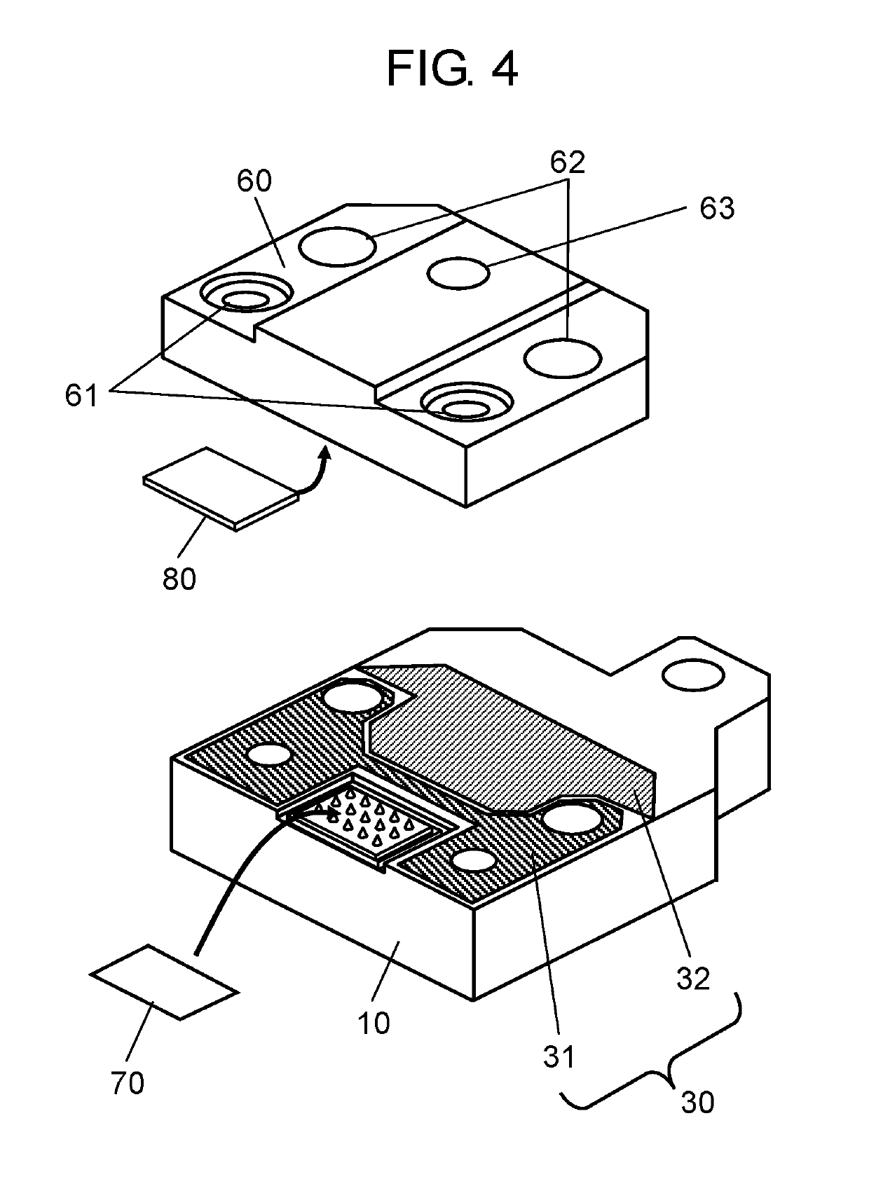
[0028]Hereinafter, a first exemplary embodiment of the present disclosure will be described with reference to FIG. 1 to FIG. 7.

[0029]FIG. 1 is a cross-sectional view illustrating a schematic configuration of semiconductor laser device 1 according to the present embodiment. FIG. 2 to FIG. 7 are perspective views illustrating a method for manufacturing semiconductor laser device 1 according to the present embodiment.

[0030]As illustrated in FIG. 1, semiconductor laser device 1 (semiconductor device) includes electrode block 10 (first electrode block), submount 20, insulating layer 30, semiconductor laser element 40 (semiconductor element), bump 50, and electrode block 60 (second electrode block). Furthermore, metal sheet 70 and metal layer 80 are provided in this order from bump 50 side between bump 50 and electrode block 60.

[0031]Electrode block 10 is electrically conductive, contains copper (Cu) as a main material, and is formed by plating a copper block with nickel (Ni) and gold (Au...

second exemplary embodiment

[0047]Next, a second exemplary embodiment of the present disclosure will be described with reference to FIG. 8 to FIG. 14. It should be noted that the same constituents as those of the first exemplary embodiment are given the same reference numerals, and the description of those constituents will be omitted. FIG. 8 is a cross-sectional view illustrating a schematic configuration of power semiconductor device 2 according to the present embodiment. FIG. 9 to FIG. 14 are perspective views illustrating a method for manufacturing power semiconductor device 2 according to the present embodiment.

[0048]In the first exemplary embodiment, semiconductor laser element 40 that outputs a laser beam is used as a semiconductor element, and semiconductor laser element 40 and submount 20 are mounted on an end portion of the upper surface of electrode block 10. By contrast, in the present embodiment, power semiconductor element 140 is used as a semiconductor element, and power semiconductor element 14...

third exemplary embodiment

[0062]Next, a third exemplary embodiment of the present disclosure will be described with reference to FIG. 15 and FIG. 16. It should be noted that the same constituents as those of the first exemplary embodiment are given the same reference numerals, and the description of those constituents will be omitted. FIG. 15 is a cross-sectional view illustrating a schematic configuration of semiconductor laser device 3 according to the present embodiment. FIG. 16 is a perspective view illustrating the schematic configuration of semiconductor laser device 3 according to the present embodiment.

[0063]In the first exemplary embodiment, recess 11 is provided in the upper surface of electrode block 10 on which submount 20 is mounted, and the lower surface of electrode block 60 facing the upper surface of electrode block 10 is flat. By contrast, in the present embodiment, the upper surface of electrode block 210 on which submount 20 is mounted is flat, and recess 261 is provided in the lower surf...


PUM


Abstract

A semiconductor device according to the present disclosure includes an electrically conductive first electrode block, an electrically conductive submount, an insulating layer, a semiconductor element, an electrically conductive bump, and an electrically conductive second electrode block. The submount is provided in a first region of the upper surface of the first electrode block, and electrically connected to the first electrode block. The semiconductor element is provided on the submount, and has a first electrode electrically connected to the submount. The bump is provided on the upper surface of a second electrode, opposite the first electrode, of the semiconductor element, and electrically connected to the second electrode. A third region of the lower surface of the second electrode block is electrically connected to the bump via an electrically conductive metal layer. An electrically conductive metal sheet is provided between the metal layer and the bump.

Description

[0001]This application is a U.S. national stage application of the PCT International Application No. PCT / JP2015 / 003933 filed on Aug. 5, 2015, which claims the benefit of priority of U.S. patent application 62 / 096,997 filed on Dec. 26, 2014, the contents all of which are incorporated herein by reference.TECHNICAL FIELD[0002]The present disclosure relates to a semiconductor device, and in particular to a semiconductor device mounted with a semiconductor element that generates much heat.BACKGROUND ART[0003]In recent semiconductor devices including a power semiconductor element or a semiconductor laser element, a larger electric current flows through the semiconductor element, and the amount of heat generated from the semiconductor element is increased accordingly. For example, in a high-power semiconductor laser device used for laser processing, a larger electric current flows through a semiconductor laser element mounted on the device in order to obtain a high-power laser beam, and th...

Claims


Application Information

Patent Timeline
Patent Type & Authority Patents(United States)
IPC IPC(8): H01S5/024H01L25/18H01S5/042H01L23/06H01L23/13H01L23/14H01L23/40H01L23/00H01S5/022H01L25/07H01L23/36H01L23/48H01L23/373H01L29/861H01S5/0233
CPCH01L23/3731H01L23/06H01L23/13H01L23/142H01L23/36H01L23/3736H01L23/4006H01L23/48H01L24/13H01L24/16H01L25/07H01L25/18H01S5/024H01S5/02236H01S5/042H01S5/0425H01L2924/16251H01L29/861H01L2023/4043H01L2023/4068H01L2224/13144H01L2224/16245H01L2924/0002H01L2924/1203H01L2924/12042H01L2924/15153H01L2924/16235H01L2924/00H01S5/02469H01S5/02492H01L2224/73253H01L2224/16227H01L2224/32245H01L2224/72H01S5/02365H01S5/023H01S5/0233H01S5/0235H01S5/0237H01S5/02345
Inventor UEDA, NAOTOOOMORI, KOUJIYOSHIDA, TAKAYUKIMOTOFUJI, TAKUMA
Owner PANASONIC INTELLECTUAL PROPERTY MANAGEMENT CO LTD
Why Eureka
Try Eureka