
Semiconductor package having reduced internal power pad pitch

a technology of power pad and package, which is applied in the direction of semiconductor devices, semiconductor/solid-state device details, electrical apparatus, etc., can solve the problems of reducing the voltage applied to transistors, generating heat during power delivery, and only supporting lateral separation pitches in flip-chip packaging technology, so as to reduce the lateral separation of ic pads/packages, reduce power and ground ir drop, and reduce the effect of ir drop

Active Publication Date: 2019-05-28
FUTUREWEI TECH INC
View PDF11 Cites 1 Cited by
  • Summary
  • Abstract
  • Description
  • Claims
  • Application Information

AI Technical Summary

Benefits of technology

The patent text describes a new structure for IC pads and package pads that reduces the distance between them, which results in a significant reduction of power and ground resistivity. This reduction helps to increase the operation speed of the transistors and reduce heating caused by power dissipation. Overall, this new structure improves the performance and reliability of packaged IC devices.

Problems solved by technology

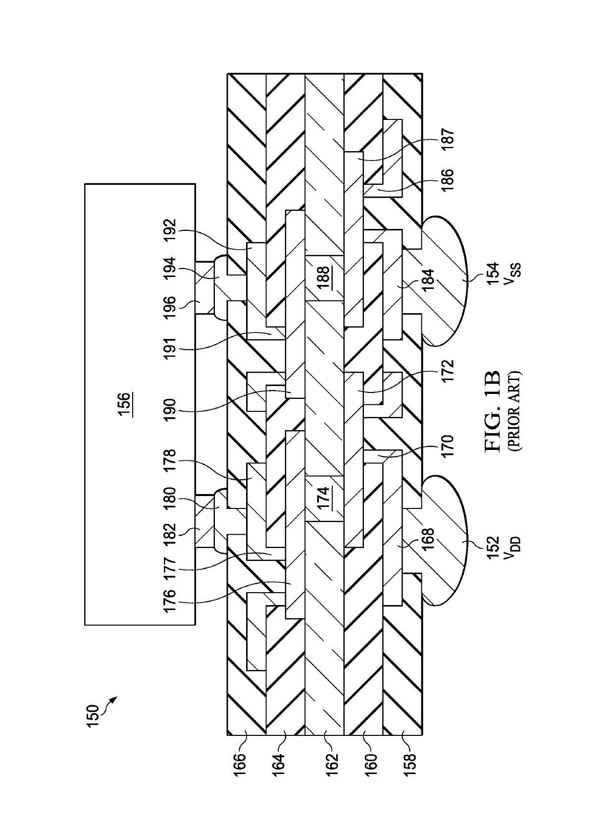
The flow of current through these patterned conductors therefore results in IR drop (voltage drop) which lowers voltage applied to transistors reducing circuit performance and generating heat during power delivery.
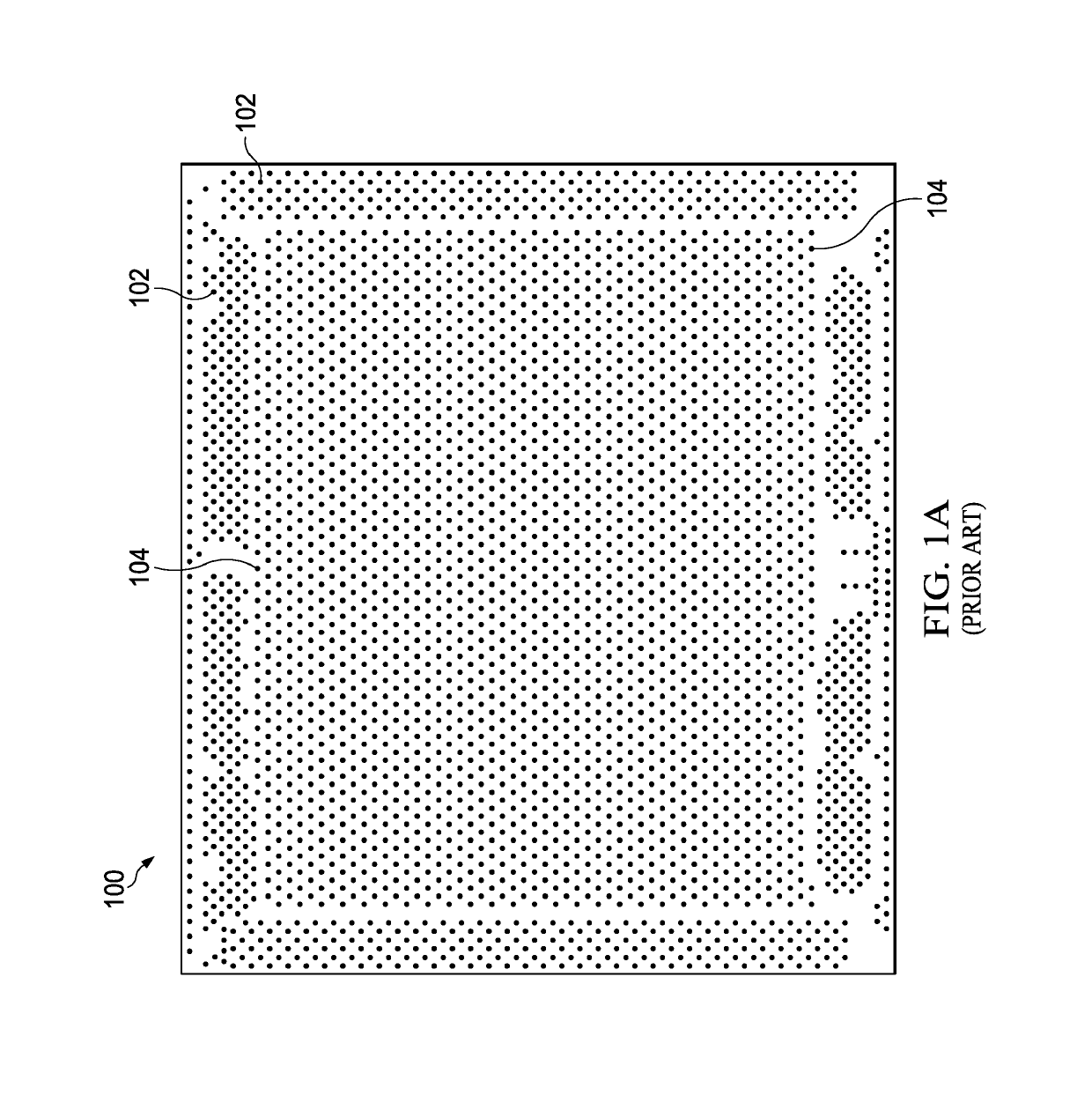
However, current flip chip packaging technology only supports lateral separation pitches between internal power / ground pads 104 down to 200 microns.
Because of this, VSS and VDD must be laterally distributed within the IC as described above, causing the problems discussed.
Such construct resulted in the distribution of power and ground within the IC greater than 200 microns from the bumps, generating heat and voltage degradation.
Further, dielectric layers of IC packages upon which the package pads were formed were typically not perfectly planar, which put stress on the ICs in response to being mounted to the IC packages.

Method used


Image

  • Semiconductor package having reduced internal power pad pitch
  • Semiconductor package having reduced internal power pad pitch
  • Semiconductor package having reduced internal power pad pitch

Examples


Embodiment Construction

[0027]It should be understood at the outset that, although illustrative implementations of one or more embodiments are provided below, the disclosed systems and / or methods may be implemented using any number of techniques, whether currently known or in existence. The disclosure should in no way be limited to the illustrative implementations, drawings, and techniques illustrated below, including the exemplary designs and implementations illustrated and described herein, but may be modified within the scope of the appended claims along with their full scope of equivalents.

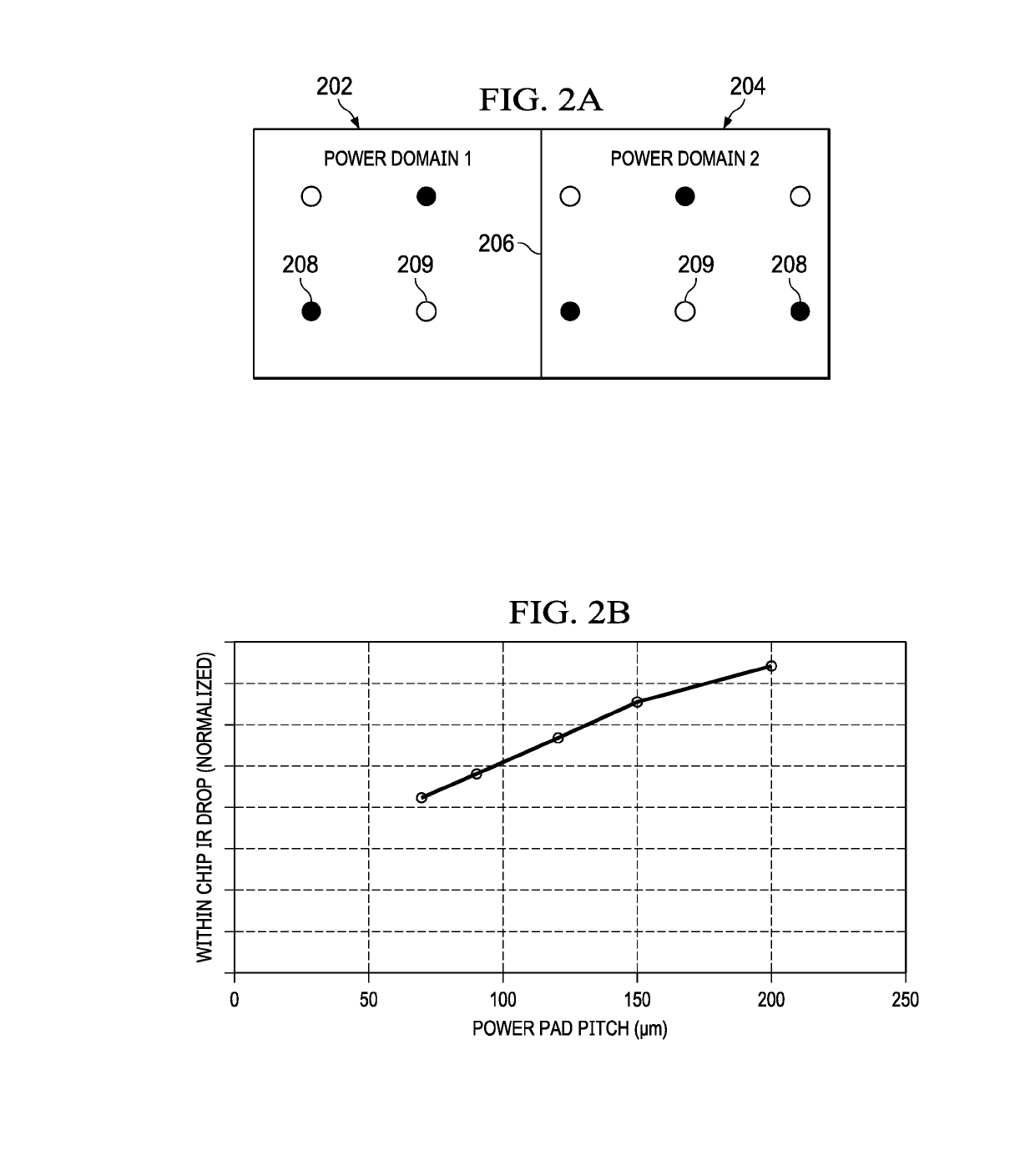
[0028]FIG. 2A is a block diagram illustrating power domains of an IC. Illustrated are a first power domain 202 and a second power domain 204. To reduce overall IC power consumption, one or both power domains 202 and 204 may be selectively shut down or operated at a reduced voltage. Also shown in FIG. 2A are power connections 208 and ground connections 209 of the IC, e.g., IC pads. The power connections 208 are shown ...


PUM


Abstract

A packaged Integrated Circuit (IC) includes an IC and a package. The package has a bottom dielectric layer and a plurality of redistribution layers (RDLs) formed on the bottom dielectric layer. Each the RDLs includes patterned conductors, a dielectric layer, and a plurality of vias that extend between the patterned conductors to a differing RDL or to external connections. The package includes a plurality of package pads that have a first lateral separation pitch. The IC includes a plurality of IC pads that electrically connect to the plurality of package pads that have a first lateral separation pitch. The package also includes a plurality of Printed Circuit Board (PCB) pads that extend through the bottom dielectric layer and contact the plurality of patterned conductors of the first RDL. Power PCB pads and ground PCB pads of the plurality of PCB pads have a second lateral separation pitch that exceeds the first lateral separation pitch.

Description

BACKGROUND OF THE INVENTION[0001]Integrated Circuit (IC) technology has advanced greatly over the past fifty years. ICs are now pervasive and present in electronic devices, machinery, vehicles, appliances, and many other devices. Large processing ICs now include billions of transistors while memory ICs include hundreds of billions of transistors. The density of transistors on ICs can reach 100 million transistors per square millimeter.[0002]Transistors of the ICs are formed in a semi conducive portion of the IC and are interconnected by patterned conductors formed in ten or more metal layers of the IC. Such interconnection of the transistors creates logic functions. The metal layers are also used to route signals within the IC, to route signals external to the IC, and to distribute supply voltages to the transistors, e.g., source supply voltage (VSS) and drain supply voltage (VDD), often referred to as power and ground, respectively. Distribution of VSS and VDD within an IC uses pat...

Claims


Application Information

Patent Timeline
Patent Type & Authority Patents(United States)
IPC IPC(8): H01L21/44H01L23/00H01L21/768
CPCH01L24/09H01L21/76843H01L21/76873H01L24/03H01L24/06H01L2924/181H01L2224/02331H01L2224/02379H01L2224/0347H01L2924/15174H01L2224/0231H01L2224/16225H01L2924/15311H01L2224/18H01L2224/81001H01L2924/14H01L2221/68345H01L2224/81192H01L2224/81385H01L2924/00014H01L24/19H01L24/20H01L24/16H01L24/81H01L23/50H01L2224/81801H01L2224/13101H01L2221/68359H01L23/3128H01L2221/68318H01L23/49816H01L23/49822H01L2224/04105H01L2224/12105H01L2224/73267H01L2224/32225H01L2224/92244H01L2924/00012H01L2224/05599H01L2924/014
Inventor GU, SHIQUNZHANG, HONGYINGCAI, HONGLIANG
Owner FUTUREWEI TECH INC
Learn More