

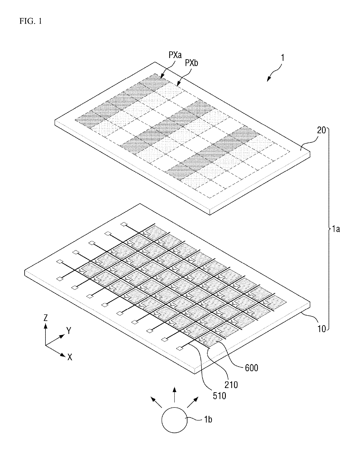
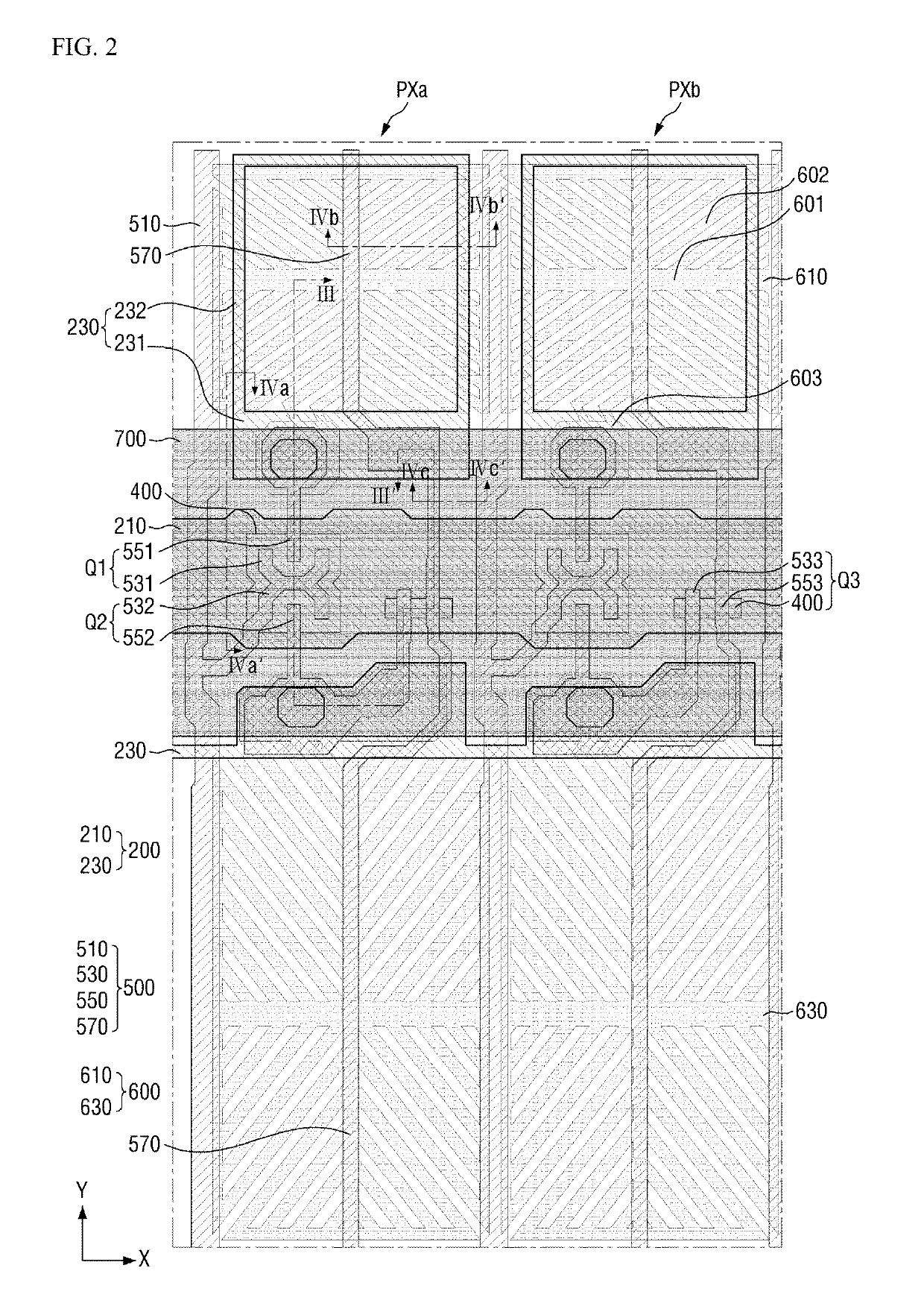
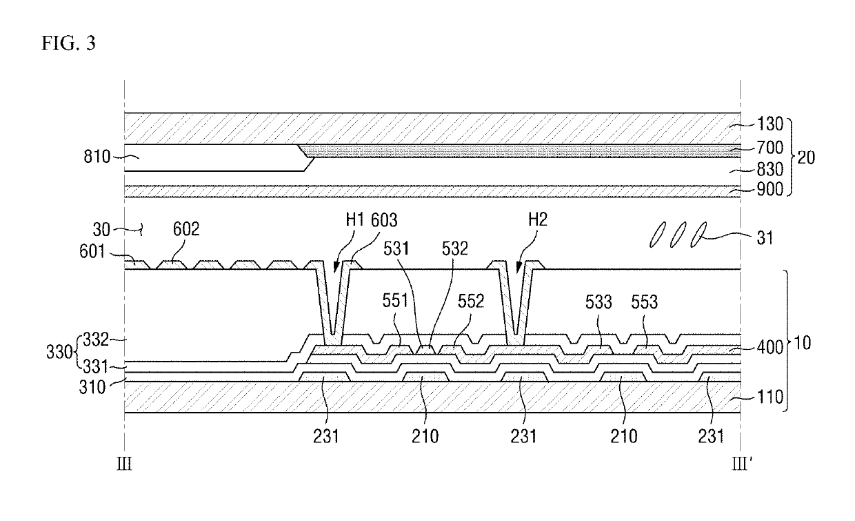
Wire substrate, display device including the same, and method of fabricating wire substrate
a display device and wire substrate technology, applied in semiconductor devices, semiconductor/solid-state device details, instruments, etc., can solve the problems of lowering the contrast of the display device, deteriorating display quality, and difficult to achieve a sufficient aperture ratio, etc., to suppress the deterioration of display quality, low reflectivity, and low reflectivity
- Summary
- Abstract
- Description
- Claims
- Application Information
AI Technical Summary
Benefits of technology
Problems solved by technology
Method used
Image

Examples
experimental example 1
ivity According to Tantalum Content
[0169]A single titanium layer was deposited on a glass substrate at the thickness of approximately 200 Å. Subsequently, a single copper layer was deposited on the titanium layer at the thickness of approximately 6,000 Å. Subsequently, a MoxTayOz target material having the content of tantalum of 1.0 at % among the metal atoms was prepared. The target material was deposited to a thickness of about 400 Å on the copper film by sputtering to prepare a triple-layer stack.
[0170]Subsequently, a photosensitive mask pattern was formed on the triple-layer stack, and the etchant was applied onto it. The etchant utilized includes peroxysulfate as the main component for etching and further includes an organic acid, a fluorine-containing compound, and a cyclic amine compound. It took 171 seconds until the etching has been completed. Here, the etch time was 171 seconds.
[0171]After the etchant was applied, images of the residual stack pattern were captured utilizin...
experimental example 2
ivity According to Tantalum Content
[0172]A triple-layer stack was prepared in substantially the same manner as in Experimental Example 1 except that the content of tantalum in the target material was 2.0 at %. Then, the etchant was applied onto the triple-layer stack. The etch time was 194 seconds.
[0173]Subsequently, images were captured by a microscope, and the tip length and reflectivity of the MoxTayOz layer were measured.
experimental example 3
ivity According to Tantalum Content
[0174]A triple-layer stack was prepared in substantially the same manner as in Experimental Example 1 except that the content of tantalum in the target material was 4.0 at %. Then, the etchant was applied onto triple-layer stack. The etch time was 295 seconds.
[0175]Subsequently, images were captured by a microscope, and the tip length and reflectivity of the MoxTayOz layer were measured.
PUM
| Property | Measurement | Unit |
|---|---|---|
| reflectivity | aaaaa | aaaaa |
| wavelength | aaaaa | aaaaa |
| melting point | aaaaa | aaaaa |
Abstract
Description
Claims
Application Information