

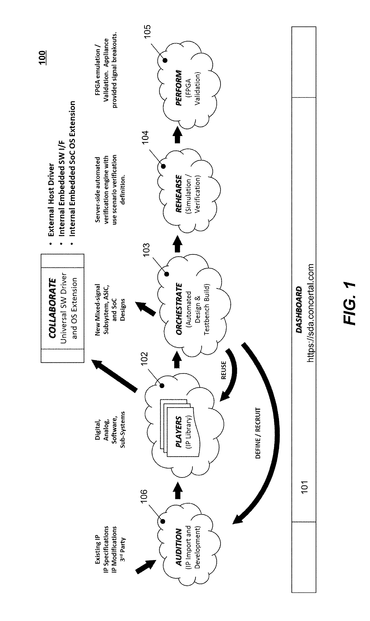
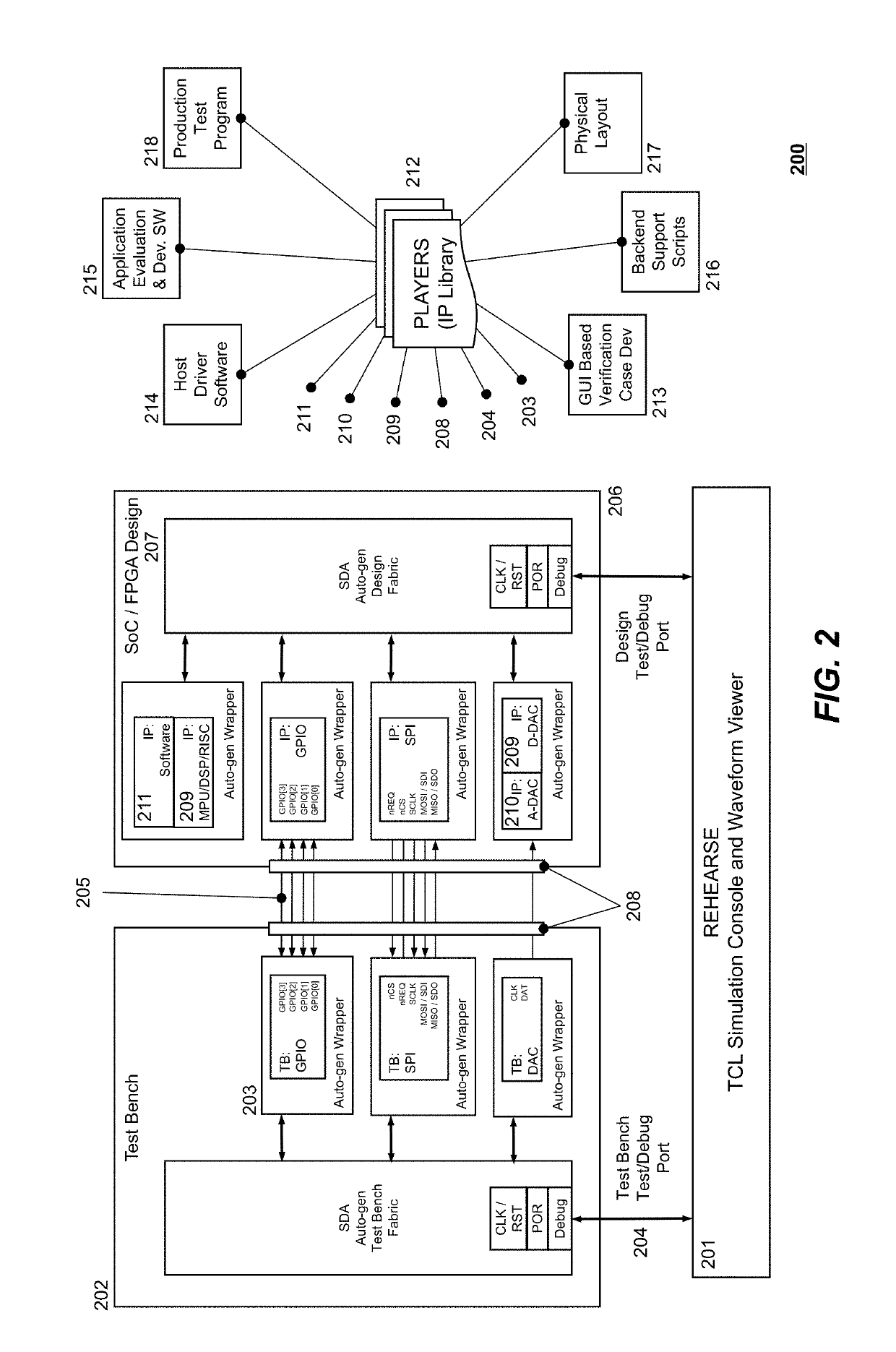
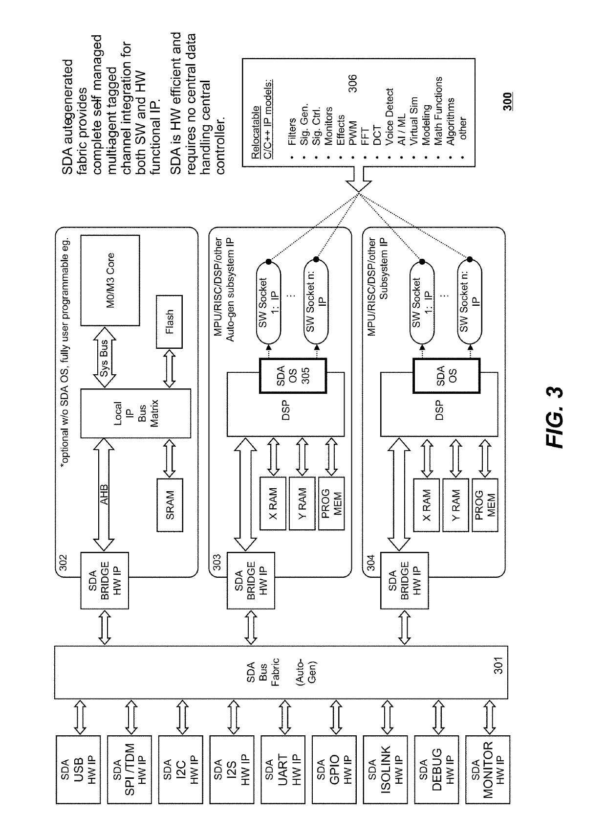
Methods and systems for system design automation (SDA) of mixed signal electronic circuitry including embedded software designs
a technology of electronic circuitry and embedded software, which is applied in the field of method and system design automation of mixed signal electronic circuitry including embedded software designs, can solve the problems of affecting the marketability of new silicon, etc., so as to facilitate automation and simplify the problem of functional integration and automation build
- Summary
- Abstract
- Description
- Claims
- Application Information
AI Technical Summary
Benefits of technology
Problems solved by technology
Method used
Image

Examples
Embodiment Construction
[0041]The detailed description set forth below in connection with the appended drawings is intended as a description of exemplary embodiments in which the presently disclosed process may be practiced. The term “exemplary” used throughout this description means “serving as an example, instance, or illustration,” and should not necessarily be construed as preferred or advantageous over other embodiments. The detailed description includes specific details for providing a thorough understanding of the presently disclosed method and system. However, it will be apparent to those skilled in the art that the presently disclosed process may be practiced without these specific details. In some instances, well-known structures and devices are shown in block diagram form in order to avoid obscuring the concepts of the presently disclosed method and system.
[0042]In the present specification, an embodiment showing a singular component should not be considered limiting. Rather, the subject matter ...
PUM
 Abstract
Description
Claims
Application Information