Transparent electrode and electronic device

a transparent electrode and electronic device technology, applied in the direction of glass/slag layered products, chemistry apparatus and processes, other domestic articles, etc., can solve the problems of high material cost, insufficient resistance reduction, and difficulty in using resin substrates at such temperature conditions, and achieve excellent transparency, low driving voltage, and high conductivity

Active Publication Date: 2020-01-14
KONICA MINOLTA INC
View PDF9 Cites 0 Cited by
  • Summary
  • Abstract
  • Description
  • Claims
  • Application Information

AI Technical Summary

Benefits of technology

[0032]The present invention may provide a transparent electrode provided with both excellent transparency and high conductivity, and the present invention may provide an electronic device equipped with this transparent electrode achieving low driving voltage and excellent color shift stability.
[0033]A formation mechanism or an action mechanism of the effects of the present invention is not clearly identified, but it is supposed as follows.
[0034]Generally, when it is produced a transparent electrode provided with sufficient conductivity and transparency by a conductive layer composed of silver as a main component, formation of a uniform thin layer is required so that the conductive layer works as an electrode. Consequently, it is necessary to make a condition of preventing formation of a non-uniform layer caused by aggregation.
[0035]However, silver atoms make thin film growth in the nucleus growth mode (Volumer-Weber (VW) mode) in general. Therefore, silver atoms are easily isolated in the shape of islands. As a result, it is difficult to obtain large conductivity when the film thickness is small, and the sheet resistance will become high. Consequently, the film thickness is required to be large for securing conductivity. The large film thickness leads to decrease of light transmittance. It was difficult to obtain a transparent electrode achieving both conductivity and light transmittance.
[0036]The present inventors found the following. By forming an organic functional layer containing a first organic compound represented by Formula (1) and a second organic compound having a different structure from a structure of the first organic compound on a substrate, or on an optical adjusting layer disposed on a substrate when needed, the conductive layer containing silver as a main component becomes to form a uniform film.
[0037]Namely, in the present invention, by using a second organic compound combined with a first organic compound represented by Formula (1) having high affinity with silver, each component of the organic functional layer will be placed in a random arrangement in the layer. That is, the component is not localized in the layer and it is placed in a uniform distribution state. As a result, the conductive layer formed on the organic functional layer becomes a continuous silver film. By forming an organic functional layer containing a first organic compound represented by Formula (1) and a second organic compound, the silver atoms will form a two-dimensional core on the organic functional layer containing a silver-affinity compound having an atom exhibiting affinity with silver atoms. A single crystal layer is formed around the two-dimensional core by film growth in the layer growth mode (Frank-van der Mere (FW) mode).

Problems solved by technology

However, when the used silver film was made thin to an extent of not inducing loss of light transmittance, the resistance did not sufficiently decrease.
Since ITO employs a rare earth metal In, the cost of material is high.
It was difficult to use a resin substrate at such temperature condition.
On the other hand, it has a problem of trade-off between resistance and light transmittance.
However, a transparent electrode composed of silver and aluminum having high electric conductivity had slightly insufficient sheet resistance.
Consequently, light transmittance will be deteriorated.
It was difficult to achieve sufficient conductivity and light transmittance at the same time.
Further, in a silver-aluminum alloy, aluminum has a property of easily oxidized.
It has a problem of increasing the resistance by oxidization.

Method used


Image

  • Transparent electrode and electronic device
  • Transparent electrode and electronic device
  • Transparent electrode and electronic device

Examples


first embodiment

[First Embodiment of Organic EL Element]

[Structure of Organic EL Element]

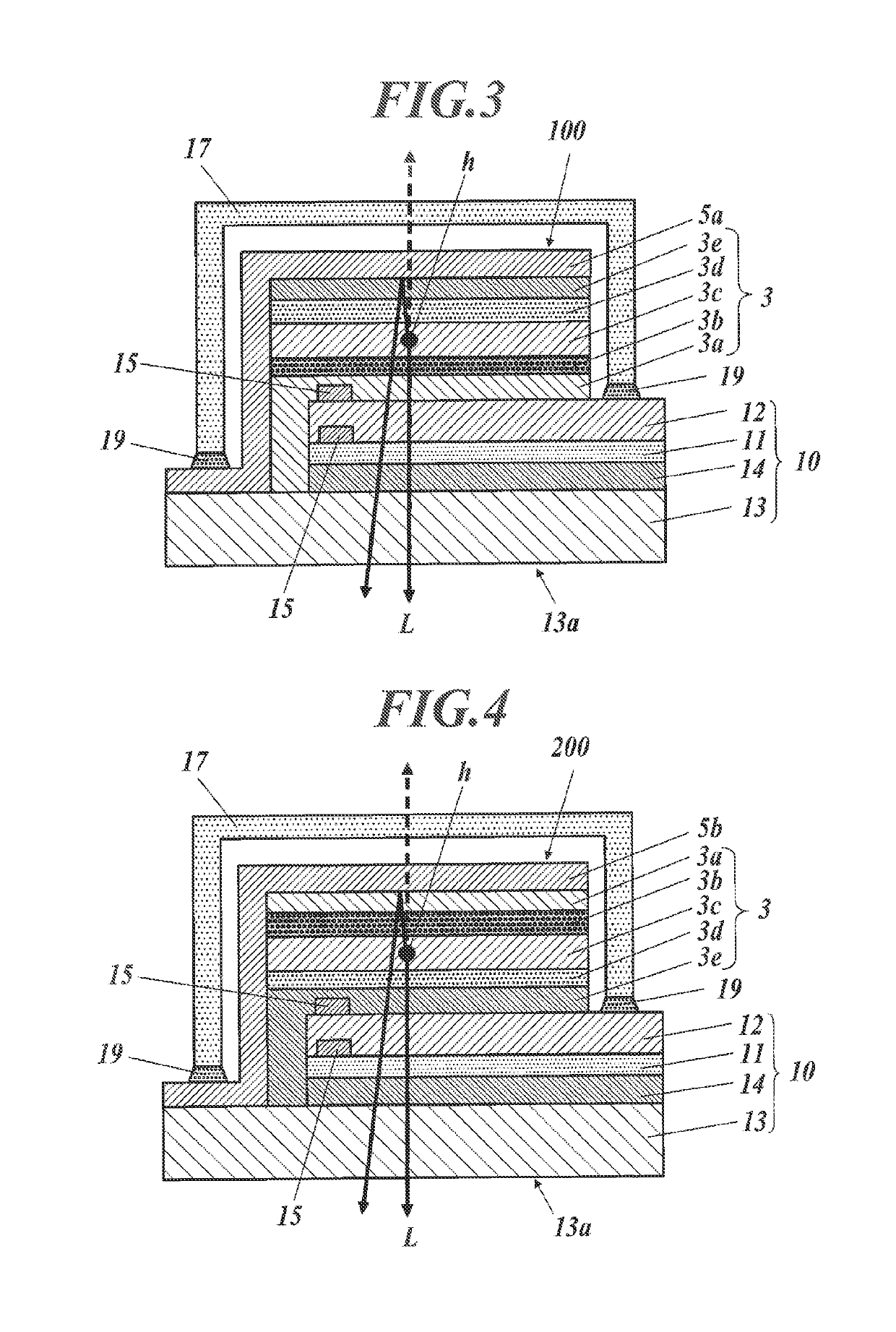
[0124]FIG. 3 is a cross sectional view illustrating the structure of a first embodiment of an organic EL element using the transparent electrode (10) of the present invention as an example of an electronic device of the present invention.

[0125]Hereinafter, the structure of the organic EL element is described with reference to FIG. 3.

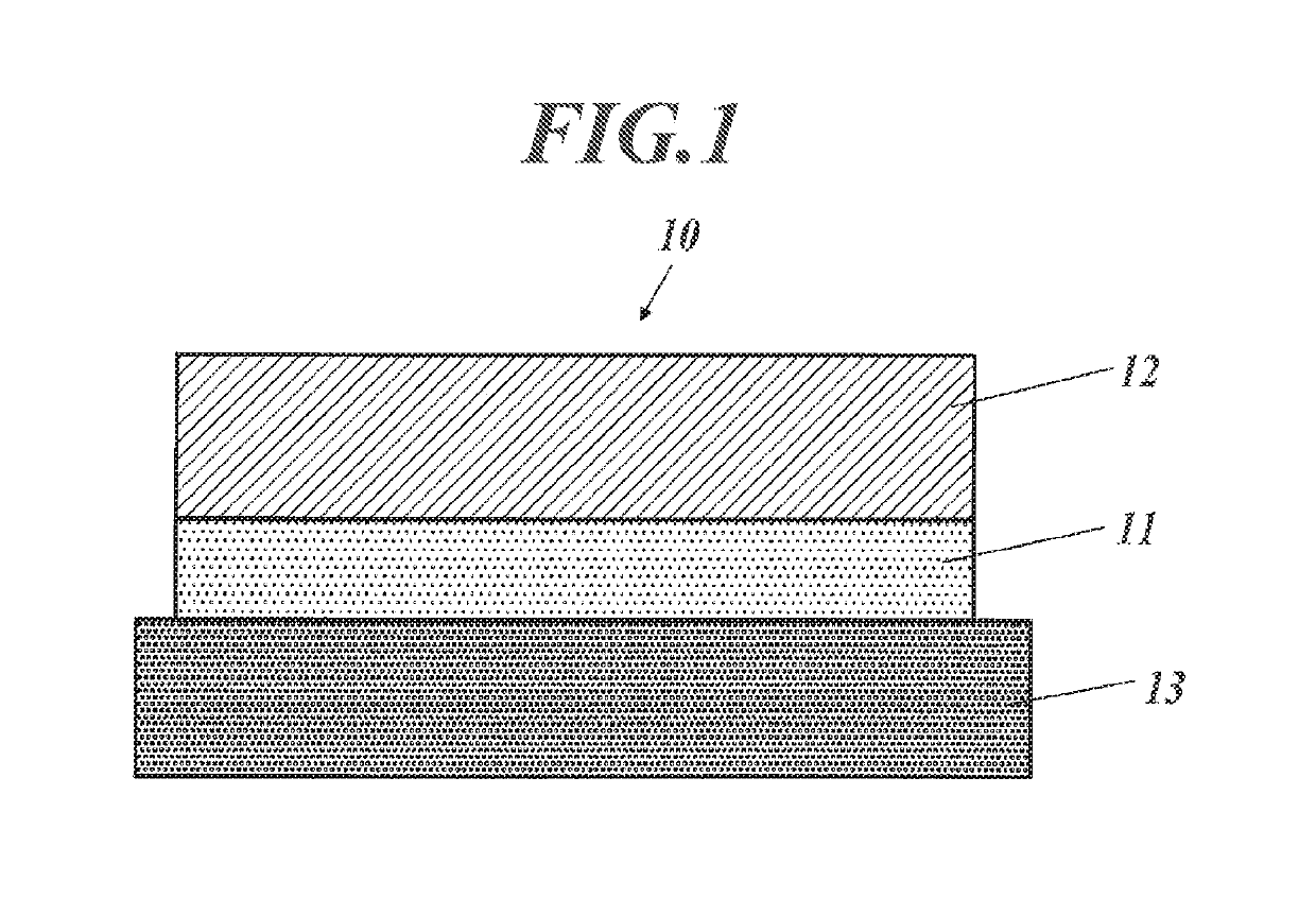
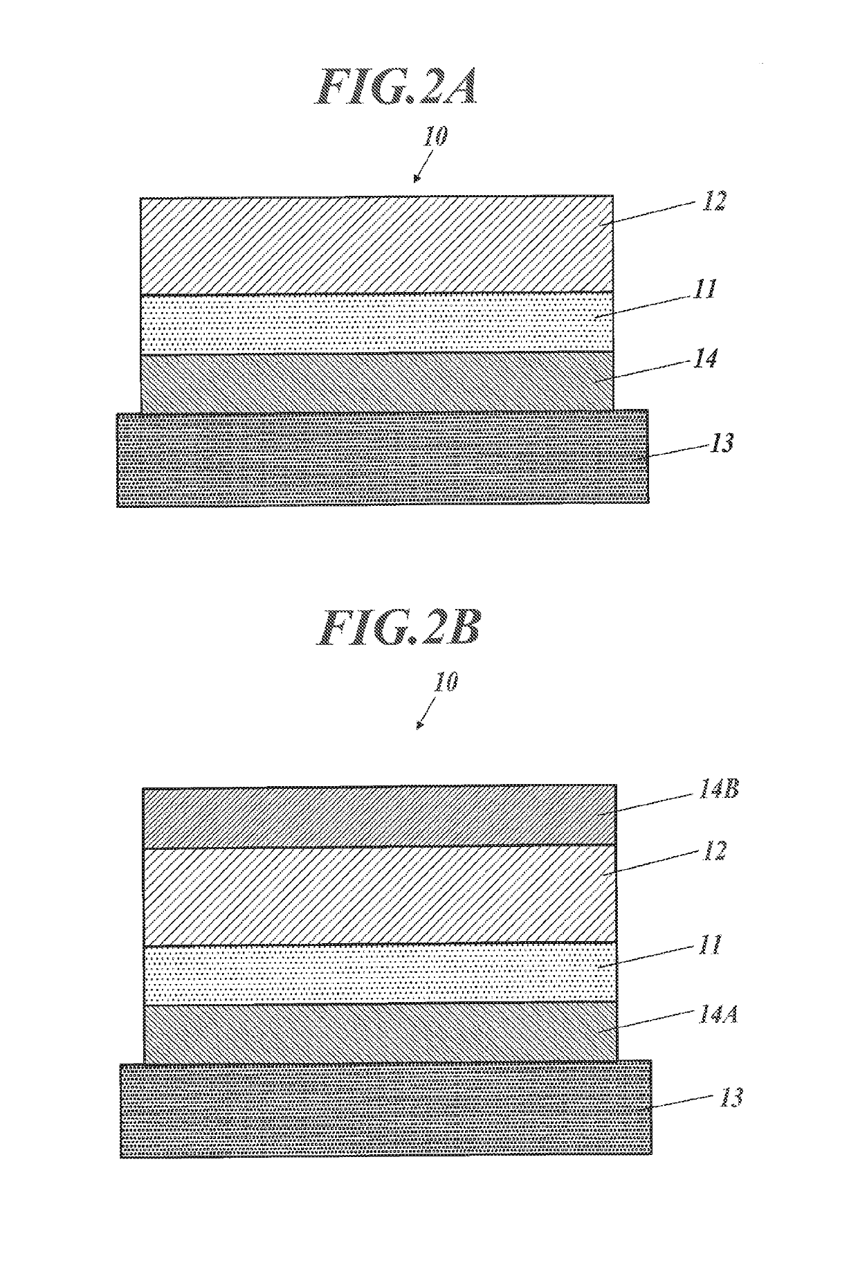
[0126]As illustrated in FIG. 3, an organic EL element (100) is disposed on a transparent substrate (13, it may be called as a base), and on the transparent substrate (13), it is disposed a transparent electrode (10) that is illustrated in FIG. 2A. On the transparent substrate that is a base (13) for the transparent electrode, there are laminated an optical adjusting layer (14), an organic functional layer (11) and a conductive layer (12). On this, there are laminated an organic light emitting layer unit (3) and a counter electrode (5a).

[0127]In this organic EL element (100), as the ...

second embodiment

[Second Embodiment of Organic EL Element]

[Structure of Organic EL Element]

[0222]FIG. 4 is a schematic cross-sectional view illustrating an organic EL element of a second embodiment using the above-described transparent electrode (10) as an example of an electronic device of the present invention. Difference between an organic EL element (200) of the second embodiment illustrated in FIG. 4 and the organic EL element (100) of the first embodiment described with reference to FIG. 3 is that the organic EL element (200) uses a transparent electrode (10) as a cathode.

[0223]Detailed description about components which are the same as those of the first embodiment is not repeated, and components specific to the organic EL element (200) of the second embodiment are described below.

[0224]As illustrated in FIG. 4, the organic EL element (200) is disposed on a transparent substrate (13), and as with the first embodiment, it uses the above-described transparent electrode (10) of the present inven...

example 1

«Production of Transparent Electrode»

[0246]As described below, transparent electrodes 101 to 121 each were produced in such a way that an area of a conductive region was 5 cm×5 cm.

[Production of Transparent Electrode 1]

[0247]A substrate composed of transparent alkali-free glass (having a thickness of 0.5 μm, in Tables 1 and 2, it is indicated simply “glass”) was fixed to a substrate holder of a vacuum deposition device (BMC-800T made of Shincron Co. Ltd.), and the substrate holder was mounted in a vacuum tank of the vacuum deposition device. In addition, silver (Ag) was placed in a tungsten resistance heating boat, and the heating boat was mounted in the vacuum tank. Next, after the pressure of the vacuum tank was reduced to 4×10⁻⁴ Pa, the resistance heating boat was electrically heated. Thus, a transparent electrode 1 having a single-layer structure composed of silver having a thickness of 10 nm was formed on the base at a deposition rate of 0.1 nm / sec to 0.2 nm / sec.

[Production of ...


PUM

PropertyMeasurementUnit
temperatureaaaaaaaaaa
light transmittanceaaaaaaaaaa
thicknessaaaaaaaaaa

Abstract

An object of the present invention is to provide a transparent electrode including a substrate having thereon a conductive layer containing silver as a main component, wherein the transparent electrode has an organic functional layer between the substrate and the conductive layer; and the organic functional layer contains a first organic compound represented by Formula (1) and a second organic compound having a different structure from a structure of the first organic compound,

Description

CROSS REFERENCE TO RELATED APPLICATION[0001]This application is a 371 of PCT / JP2016 / 052942 filed on Feb. 1, 2016, which, in turn, claimed the priority of Japanese Patent Application No. 2015-037712 filed on Feb. 27, 2015, both applications are incorporated herein by reference.TECHNICAL FIELD[0002]The present invention relates to a transparent electrode and an electronic device. More specifically, the present invention relates to a transparent electrode provided with both transparency and conductivity, and an electronic device equipped with this transparent electrode.BACKGROUND[0003]A transparent electrode is generally used for: a liquid crystal display, an electroluminescent display, a plasma display, an electrochromic display, a solar battery, a touch panel, and an electronic paper.[0004]An organic EL element (it may be called as an organic-field light-emitting element), which utilizes electroluminescence (hereinafter, it is abbreviated as “EL”) of an organic material, has a config...

Claims


Application Information

Patent Timeline
Patent Type & Authority Patents(United States)
IPC IPC(8): H01L51/52B32B15/08
CPCH01L51/5215B32B15/08B32B2307/412B32B2457/00H05B33/28B32B7/12B32B17/06H10K50/816
Inventor FURUKAWA, SHUNKOJIMA, SHIGERUYOSHIDA, KAZUHIROHAKII, TAKESHI
Owner KONICA MINOLTA INC
Why Eureka
Try Eureka