Optical film, multilayer optical film including same, and method for producing optical film

a multi-layer optical film and optical film technology, applied in the field of optical films, can solve the problems of insufficient consideration of the change in the retardation due to the wavelength, difficulty in producing a film with a sufficiently small in-plane retardation, and difficulty in obtaining a film with good appearance, etc., to achieve the effect of less change in the retardation, less wavelength change, and easy production

Active Publication Date: 2020-05-12
MITSUBISHI GAS CHEM CO INC +1
View PDF50 Cites 0 Cited by
  • Summary
  • Abstract
  • Description
  • Claims
  • Application Information

AI Technical Summary

Benefits of technology

[0026]According to the present invention, a film with small in-plane retardation Re and large thickness-direction retardation Rth can inexpensively and easily be produced, and the produced optical film can compensate the viewing angle upon combining with a VA mode liquid crystal or other retardation film.
[0027]In addition, since a multilayer optical film that has less change in the retardation due to the wavelength, or that can make retardation at a lower wavelength to be smaller can be obtained, the present invention can provide a multilayer optical film that is useful in the market for thin-type display products, typically, liquid crystal televisions.

Problems solved by technology

According to a method for producing a thin film described in Patent literature 1, there is a part where the film does not make contact with the touch roller, and thus it is difficult to obtain a film with good appearance.
Moreover, even the above-described touch roller molding that uses the elastic metal roller has difficulty in producing a film with sufficiently small in-plane retardation.
For such conventional films, however, change in the retardation due to the wavelength has not fully been considered.
In addition, the thickness-direction retardation Rth as well has not been considered upon designing.

Method used


Image

  • Optical film, multilayer optical film including same, and method for producing optical film
  • Optical film, multilayer optical film including same, and method for producing optical film
  • Optical film, multilayer optical film including same, and method for producing optical film

Examples


example 1

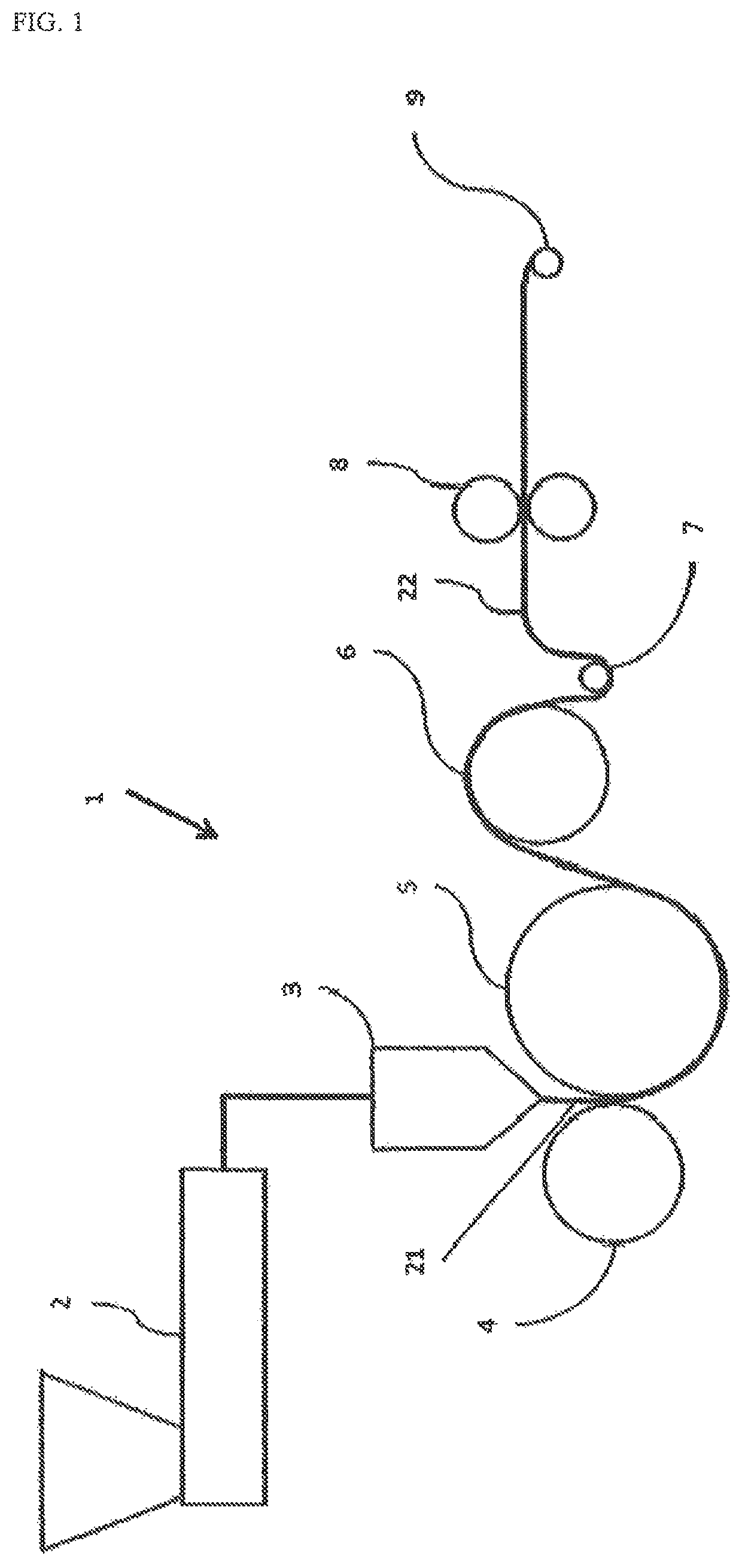
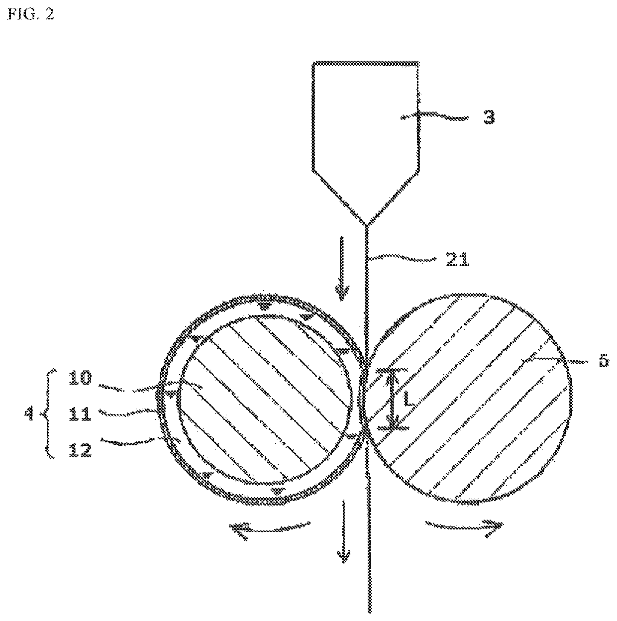
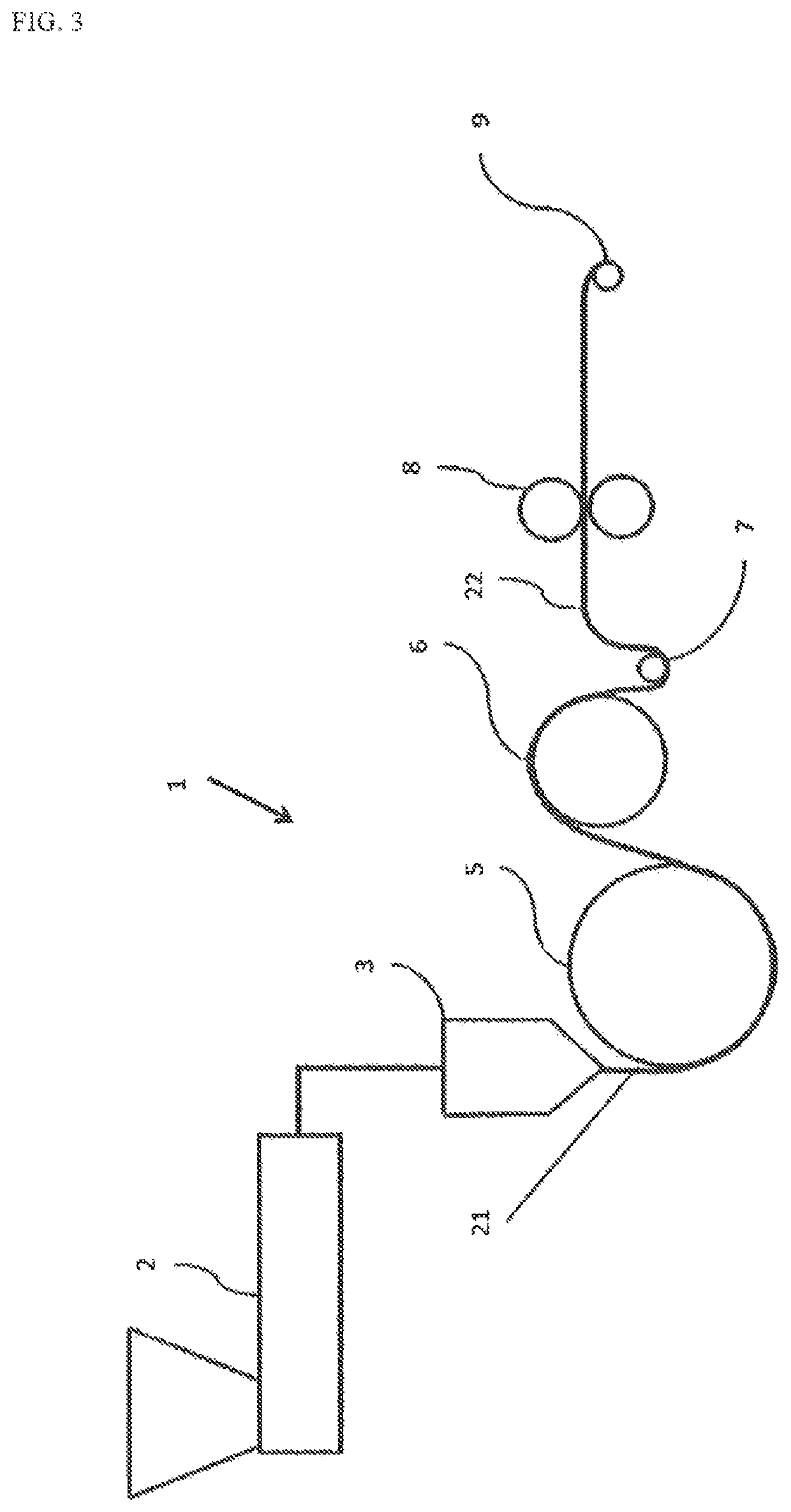
[0110]Iupilon H4000, a bisphenol A polycarbonate with a viscosity-average molecular weight of 14000-17000, was used to mold a transparent polycarbonate film with a thickness of 100 μm by a melt extrusion method via a T-die as shown in FIG. 1 at a molding temperature of 270° C., which was fed at about 260° C. and cooled between an elastic metal roller with a diameter of 300 mm and a metal roller with a diameter of 400 mm at 135° C. with a gap of 100 μm therebetween to obtain a film with a thickness of 100 μm. At this point, the linear pressure on the molten polycarbonate resin at the center parts of the two cooling rollers was 15 kgf / cm and the take-up speed was 14.5 m / min. In addition, since the thermal deformation temperature (Th) of the polycarbonate resin was 124° C., the difference from the surface temperature (Tr) of the roller was 11° C.

example 2

[0154]28 parts by mass of a polyphenylene ether-based resin (PPE) (trade name: PX100L manufactured by Mitsubishi Engineering-Plastics Corporation) and 72 parts by mass of general grade polystyrene (GPPS) (trade name: HH105 manufactured by PS Japan Corporation) were mixed to obtained a total of 100 parts by mass of a positive birefringent material, which was used to produce a film with a thickness of 200 μm by using a film prototyping device equipped with a T-die at 290° C. The prepared film was heated to 125° C. and uniaxially stretched at a stretch ratio of 2.3 times to obtain a film (film 2). The resulting sample and the film (film 1) described in Reference example below were layered using an adhesive. The evaluation results of the optical properties are shown in Table 2.

Reference Example

[0155]A film (film 1) with a thickness of 100 μm was prepared in the same manner as Example 1.


PUM

PropertyMeasurementUnit
wavelengthaaaaaaaaaa
thicknessaaaaaaaaaa

Abstract

Provided are: an optical Elm that has a good appearance, small in-plane retardation Re, and large thickness-direction retardation Rth; and a method for producing such an optical film. Also provided is a multilayer optical film that uses the optical film, that exhibits little change in retardation as a result of wavelength, and that has small retardation at low wavelengths. The optical film is obtained by sandwiching a melted resin between a first cooling roll comprising an elastic metal roll and a second cooling roll comprising a non-elastic metal roll and molding said melted resin. The optical film has a good appearance, the absolute value of the in-plane retardation Re thereof is 10 nm or less, and the thickness-direction retardation Rth thereof is 40 nm or more.

Description

TECHNICAL FIELD[0001]The present invention relates to an optical film that can be used for optical use, flat panel display use and the like, and a method for producing the same. More particularly, the present invention relates to an optical film that has small in-plane retardation Re and large thickness-direction retardation Rth which can be obtained, for example, by melt extrusion molding, and a method for producing the same. The present invention also relates to a multilayer optical film obtained by layering the above-described optical film as a retardation film.BACKGROUND ART[0002]Recently, for optical use and liquid crystal display use, an optical film that has excellent transparency and small in-plane retardation Re has been needed. In a VA mode liquid crystal cell, the refractive index in the direction vertical to the screen (thickness direction) is greater than the refractive index in the in-plane direction. Therefore, in order to improve the viewing angle in the VA mode, a f...

Claims


Application Information

Patent Timeline
Patent Type & Authority Patents(United States)
IPC IPC(8): G02B5/30B29C48/305B29C48/30B29C48/88B29D11/00B29C48/08B29C48/92B32B27/00B32B27/36B29C41/24B32B27/30B32B7/02B29C48/00B29K101/12B29K105/00
CPCB32B7/02B29C48/914B32B27/00G02B5/3083B29C48/305B29C48/92B32B27/36B29C41/24B29C48/30B32B27/30B29D11/00788B29C48/08B29C48/0011B29K2101/12B29K2105/0005B29C48/0018B29K2995/0018G02F2413/11B29C48/40G02F1/133634
Inventor KAKINOKI, OSAMUKOMURO, KOJI
Owner MITSUBISHI GAS CHEM CO INC
Why Eureka
Try Eureka