GaN-based bidirectional switch device

a switch device and bidirectional technology, applied in the field of gan-based bidirectional switch devices, can solve the problems of increasing bidirectional switch losses more power, and high on-state voltage drop, and achieves low on-state resistance, the ability to block off the device, and the utilization rate of chip area high

Active Publication Date: 2020-06-02
UNIV OF ELECTRONICS SCI & TECH OF CHINA
View PDF7 Cites 3 Cited by
  • Summary
  • Abstract
  • Description
  • Claims
  • Application Information

AI Technical Summary

Benefits of technology

[0006]In view of the main indexes of high-efficiency power switching devices (chip area utilization, on-state resistance, reverse resistance, and power consumption), the GaN-based bidirectional switch device is proposed. The present invention has the advantages of high utilization of chip area, low on-state resistance, high reverse blocking ability, and low power consumption, especially in matrix converters.
[0012]It is important to note that the ability to block off the device can be increased by increasing the depth that the insulated gate electrode is embedded in the AlGaN layer's surface.
[0013]The benefit of the present invention is that, compared with the traditional structure, the device of the present invention has the advantages of high utilization ratio of chip area, low on-state resistance, high reverse blocking ability, and low power consumption, especially in matrix converters. Due to the only presence of Schottky in this invention, no heavy elements such as gold is required, so the present invention is compatible with traditional CMOS technology.

Problems solved by technology

In this configuration, the current flows through two different devices, this will lead to a high on-state voltage drop, making the bidirectional switches lose more power.
But the new configuration goes against chip-area utilization, because only one of the two current channels can conduct currents in the bidirectional conducting mode.

Method used


Image

  • GaN-based bidirectional switch device
  • GaN-based bidirectional switch device
  • GaN-based bidirectional switch device

Examples


Embodiment Construction

[0025]The technical scheme of the invention is described in detail below.

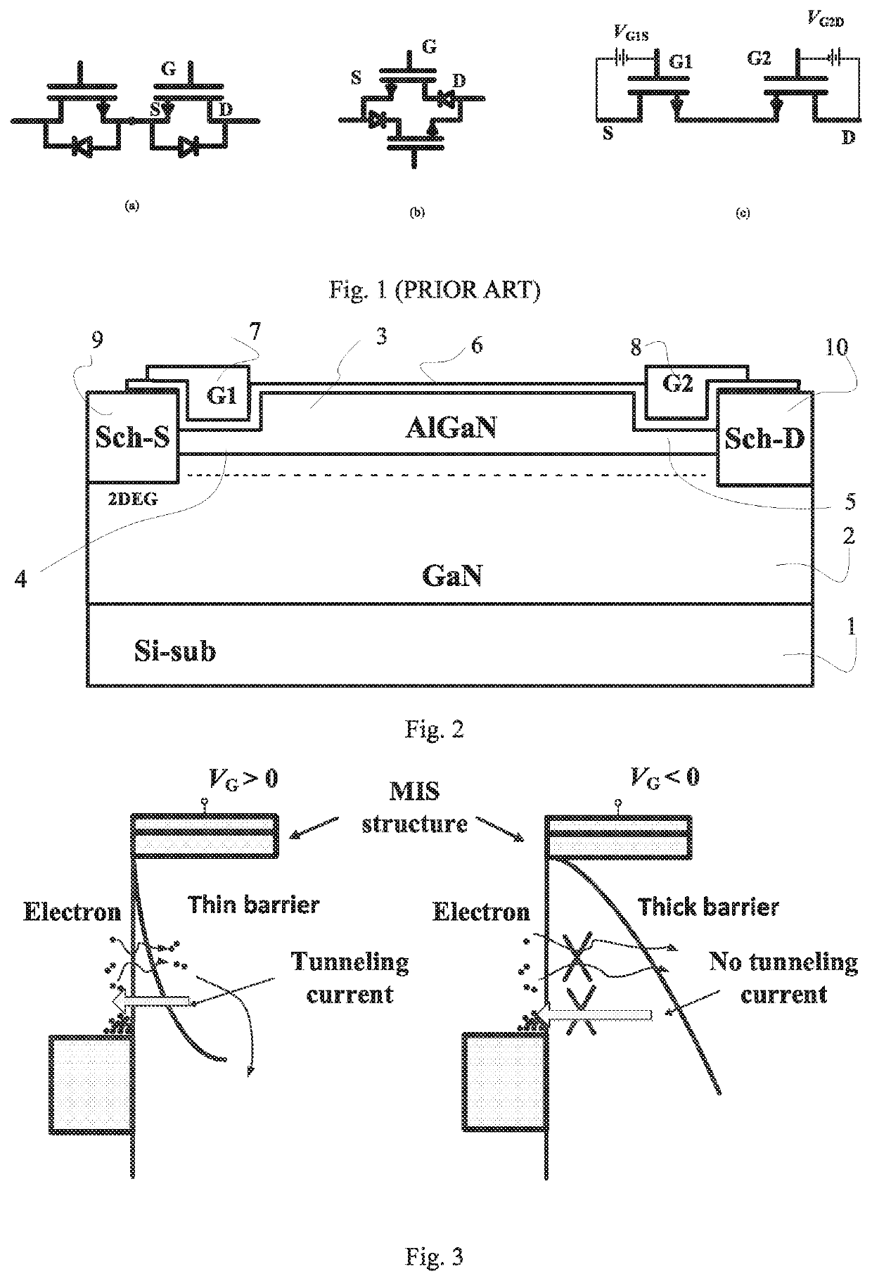
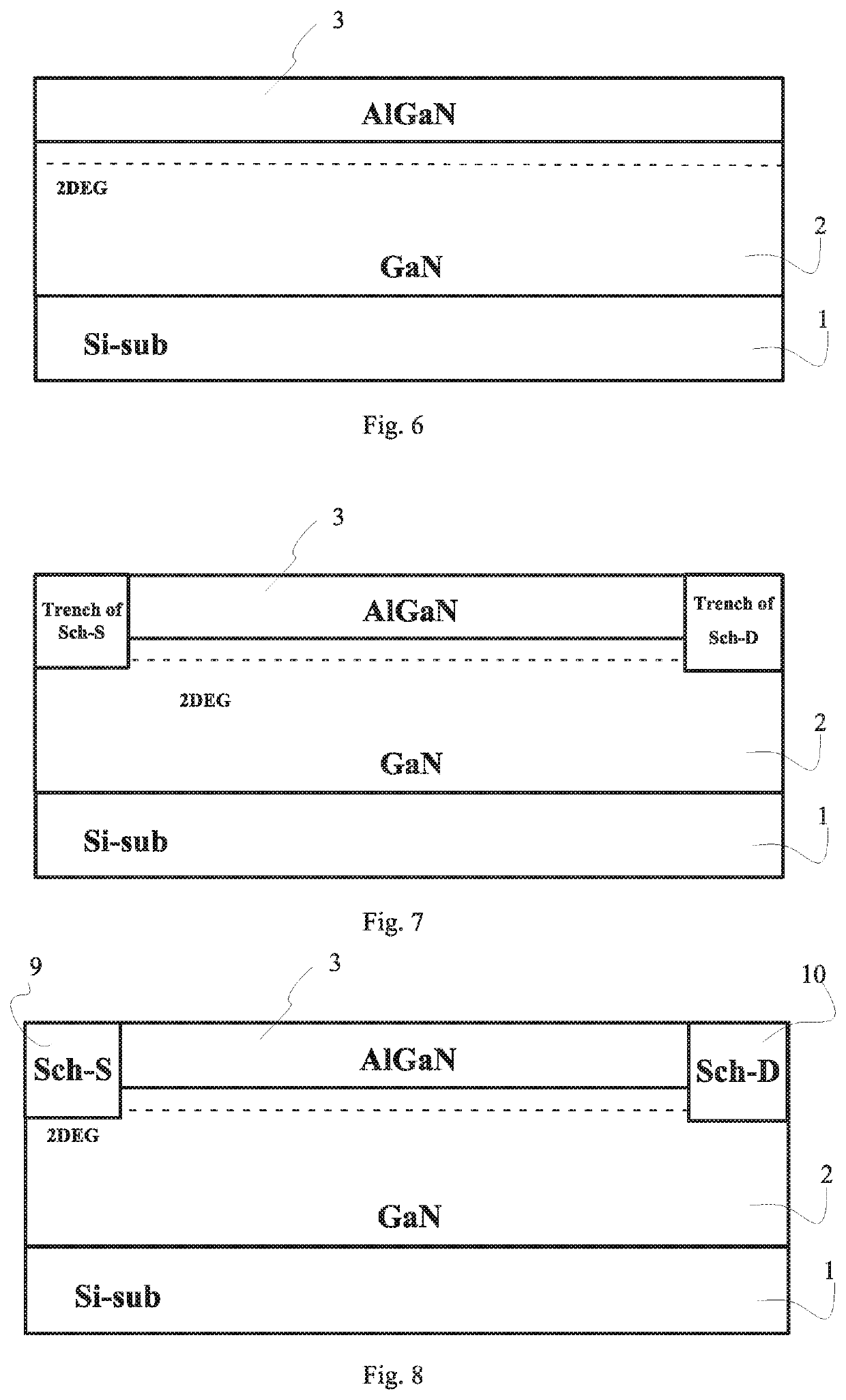
[0026]As shown in FIG. 2, the GaN-based bidirectional switch device comprises a substrate 1, a GaN buffer layer 2, an AlGaN layer 3. The GaN buffer layer 2 and the AlGaN layer 3 form a heterojunction. A Schottky source electrode structure is located at one end of the GaN-based bidirectional switch device, and a Schottky drain electrode structure is located at an other end of the GaN-based bidirectional switch device. The Schottky source electrode structure and the Schottky drain electrode structure are symmetrical with respect to a median vertical line of the GaN-based bidirectional switch device. The Schottky source electrode structure has a grooved Schottky structure, which comprises a recessed trench formed by etching the AlGaN layer 3 and a part of the GaN buffer layer 2 and a source Schottky-contact electrode 9 contacting with the GaN buffer layer 2 and covering the recessed trench of the Schottky source e...


PUM

PropertyMeasurementUnit
depthaaaaaaaaaa
electron mobilityaaaaaaaaaa
thicknessaaaaaaaaaa

Abstract

The present invention relates to the field of semiconductor switches, and relates more particularly to a GaN-based bidirectional switch device. The present invention provides a gate-controlled tunneling bidirectional switch device without Ohmic-contact, which avoids a series of negative effects (such as current collapse, incompatibility with traditional CMOS process) caused by the high temperature ohm annealing process. Each insulated gate structure near schottky-contact controls the band structure of the schottky-contact to change the working state of the device, realizing the bidirectional switch's ability of bidirectional conducting and blocking. Due to the only presence of schottky in this invention, no heavy elements such as gold is needed, and this device is compatible with traditional CMOS technology.

Description

CROSS REFERENCE[0001]The present application is based on, and claims priority from, Chinese application number 201611095490.3, filed on Dec. 2, 2016, the disclosure of which is hereby incorporated by reference herein in its entirety.TECHNICAL FIELD[0002]The present invention relates to the technical field of semiconductor switches, more particularly, to a GaN-Based bidirectional switch device.BACKGROUND[0003]Bidirectional switches, capable of conducting currents and blocking voltages of both polarities, are wildly used in many applications, such as compact motor drives, aircrafts, AC power supply units, electric propulsion of ships, and electric cars. Conventional high-voltage bidirectional switches are constructed by two Si-based insulated gate bipolar translators (IGBTs) connected in reversed series and two power diodes, as shown in FIG. 1(a). In this configuration, the current flows through two different devices, this will lead to a high on-state voltage drop, making the bidirect...

Claims


Application Information

Patent Timeline
Patent Type & Authority Patents(United States)
IPC IPC(8): H01L29/205H01L29/20H01L29/739H01L29/51H01L29/417H01L29/423H01L29/66H01L29/778
CPCH01L29/41766H01L29/205H01L29/66462H01L29/2003H01L29/7393H01L29/7786H01L29/4236H01L29/517H01L29/41725H01L29/47H01L29/772H01L29/78H01L29/7831
Inventor CHEN, WANJUNSHI, YIJUNLIU, JIECUI, XINGTAOHU, GUANHAOLIU, CHAOZHOU, QIZHANG, BO
Owner UNIV OF ELECTRONICS SCI & TECH OF CHINA
Why Eureka
Try Eureka