Method of fabricating high voltage semiconductor devices with JFET regions containing dielectrically isolated junctions

a dielectric isolation and high-voltage semiconductor technology, applied in the field of high-voltage field-effect transistors, can solve the problems of increasing the voltage-blocking capability, affecting the manufacture of devices, and buried layers tending to diffuse outwards,

Inactive Publication Date: 2010-01-28
ALPHA & OMEGA SEMICON INC
View PDF3 Cites 2 Cited by
  • Summary
  • Abstract
  • Description
  • Claims
  • Application Information

AI Technical Summary

Benefits of technology

[0019]The use of JFET regions according to this invention provides for a very efficient use of the lateral area of the chip and allows the doping concentration of the drift region to be higher than it would be if the JFET regions were not present.

Problems solved by technology

This increased voltage-blocking capability comes at a price, however.
Despite efforts to restrict the dopant to the desired location within the substrate, however, in practice the charge in the buried layers tends to diffuse outwards in three dimensions (both laterally and vertically), particularly if the device is subjected to any thermal processing after the buried layers are implanted.
This outdiffusion of dopant makes the device difficult to manufacture.
Nonetheless, all of these known charge control methods encounter problems with the dimensional control of PN junctions, especially junctions of the P-type dopant boron, during the subsequent process steps.

Method used


Image

  • Method of fabricating high voltage semiconductor devices with JFET regions containing dielectrically isolated junctions
  • Method of fabricating high voltage semiconductor devices with JFET regions containing dielectrically isolated junctions
  • Method of fabricating high voltage semiconductor devices with JFET regions containing dielectrically isolated junctions

Examples


Embodiment Construction

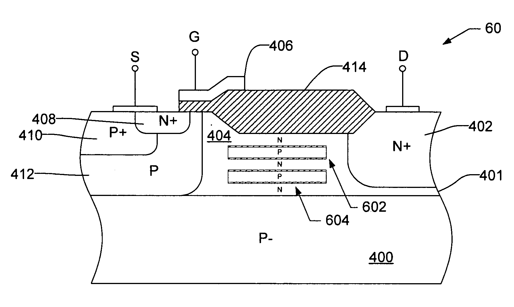
[0042]FIG. 4 is a top view of a first embodiment according to the invention. FIG. 5A is a cross-sectional view taken at cross-section 5A-5A in FIG. 4. FIG. 5B is a cross-sectional view taken at cross-section 5B-5B in FIG. 4. FIG. 6 is a cross-sectional view taken at cross-section 6-6 in FIG. 4.

[0043]Referring first to FIG. 4, a top view of a MOSFET 40 is shown. In layout, MOSFET 40 is generally of a rectangular shape, with rounded corners. As shown in FIGS. 5A and 5B, MOSFET 40 is formed in an N-epitaxial (epi) layer 401 that overlies a P− substrate 400. An N+ drain region 402 is located at the center of the rectangle, and it is surrounded by an N+ source region 408. Overlying the surface of N-epi layer 401 is a gate 406, which also surrounds N+ drain region 402. Lying outward of N+ source region 408 is a P+ body contact region 410. As shown in FIG. 5A, a P body region 412 is formed adjacent to N+ source region 408, and a channel region 417 within P body region 412 directly underlie...


PUM


Abstract

A high-voltage field-effect device contains an extended drain or “drift” region having a plurality of JFET regions separated by portions of the drift region. Each of the JFET regions is filled with material of an opposite conductivity type to that of the drift region, and at least two sides of each JFET region is lined with an oxide layer. In one group of embodiments the JFET regions extend from the surface of an epitaxial layer to an interface between the epitaxial layer and an underlying substrate, and the walls of each JFET region are lined with an oxide layer. When the device is blocking a voltage in the off condition, the semiconductor material inside the JFET regions and in the drift region that separates the JFET regions is depleted. This improves the voltage-blocking ability of the device while conserving chip area. The oxide layer prevents dopant from the JFET regions from diffusing into the drift region and allowing the JFET regions to be accurately located in the drift region.

Description

CROSS-REFERENCE TO RELATED APPLICATION[0001]This application is a divisional of application Ser. No. 11 / 157,601, filed Jun. 21, 2005, now U.S. Pat. No. ______, which is incorporated herein by reference in its entirety.FIELD OF THE INVENTION[0002]This invention relates to high voltage devices and in particular to a high-voltage field-effect transistor such as a metal-oxide-silicon field-effect transistor or an insulated gate bipolar transistor.BACKGROUND[0003]In the field of field-effect transistors there is a continual quest for devices that approximate an ideal switch, that is, devices that have a very low-resistance when they are turned on and a high voltage-blocking capability when they are turned off. Another objective is a size that occupies minimal “real estate” on today's miniaturized semiconductor chips.[0004]In accordance with the Reduced Surface Field (RESURF) principle, it is known to provide an extended “drift” region in a field-effect transistor, which in a MOSFET is an...

Claims


Application Information

Patent Timeline
Patent Type & Authority Applications(United States)
IPC IPC(8): H01L21/336
CPCH01L29/0634H01L29/0653H01L29/0696H01L29/42368H01L29/66681H01L29/7393H01L2924/0002H01L29/7816H01L29/8611H01L2924/00
Inventor YILMAZ, HAMZA
Owner ALPHA & OMEGA SEMICON INC
Why Eureka
Try Eureka