

Etching methods
a technology of etching process and substrate, applied in the direction of electrical apparatus, basic electric elements, electric discharge tubes, etc., can solve the problems of limiting the further development of advanced devices, the etching process used to fabricate such devices is often a limiting factor in the field of methods and apparatus for etching substrates
- Summary
- Abstract
- Description
- Claims
- Application Information
AI Technical Summary
Benefits of technology
Problems solved by technology
Method used
Image

Examples
Embodiment Construction
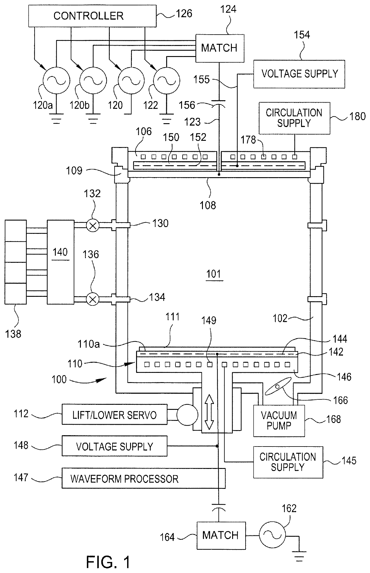
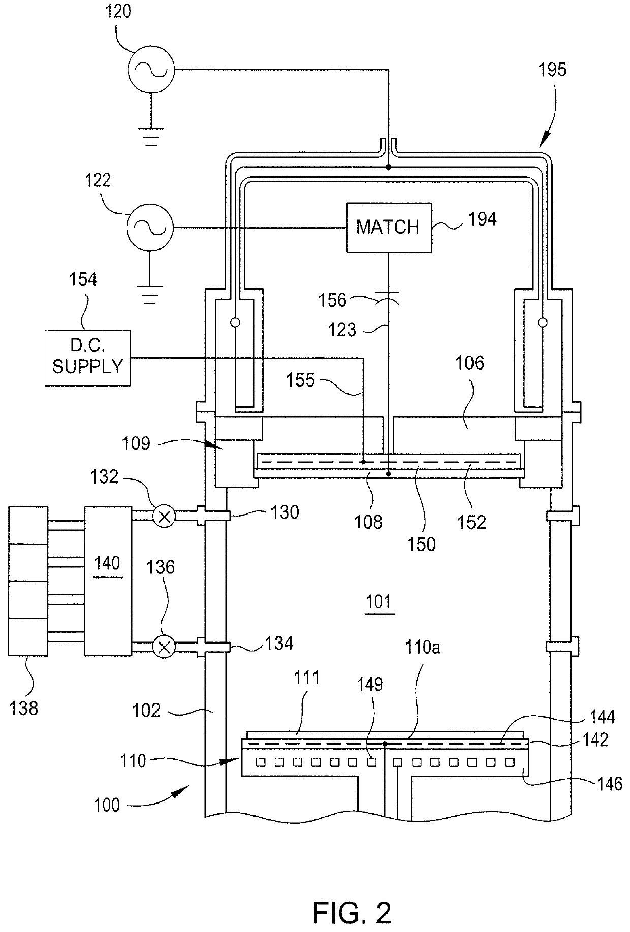
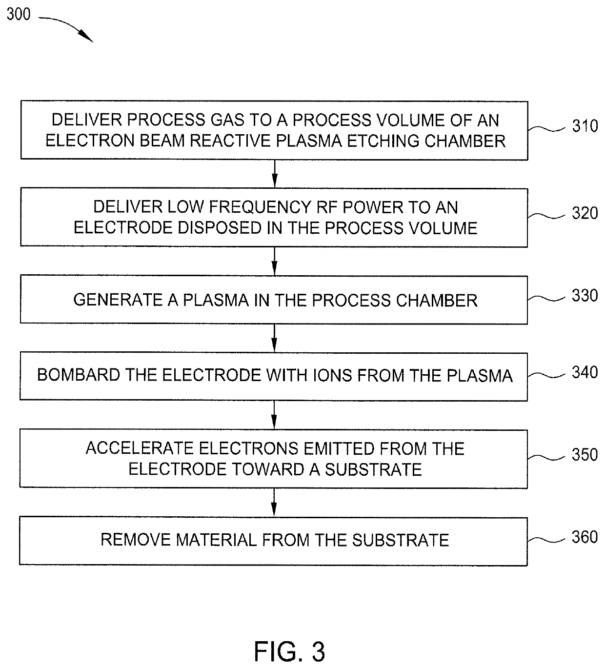
[0019]Embodiments described herein relate to apparatus and methods for performing electron beam reactive plasma etching (EBRPE). In one embodiment, an apparatus for performing EBRPE processes includes an electrode formed from a material having a high secondary electron emission coefficient. In another embodiment, methods for etching a substrate include generating a plasma and bombarding an electrode with ions from the plasma to cause the electrode to emit electrons. The electrons are accelerated toward a substrate to induce etching of the substrate.
[0020]FIG. 1 schematically illustrates an electron beam reactive plasma etching (EBRPE) chamber 100. The chamber 100 has a chamber body 102 which defines a process volume 101. In one embodiment, the chamber body 102 has a substantially cylindrical shape. In other embodiments, the chamber body 102 has a polygonal shape, such as a cubic shape or the like. The chamber body 102 is fabricated from a material suitable for maintaining a vacuum p...
PUM
| Property | Measurement | Unit |
|---|---|---|
| frequency | aaaaa | aaaaa |
| pressure | aaaaa | aaaaa |
| pressure | aaaaa | aaaaa |
Abstract
Description
Claims
Application Information