Supercharge Your Innovation With Domain-Expert AI Agents!

Method for polishing silicon wafer and surface treatment composition

a technology of silicon wafer and surface treatment composition, which is applied in the direction of cleaning with liquids, manufacturing tools, lapping machines, etc., can solve the problems of insufficient coping and adversely affecting the performance of semiconductor devices, and achieve the effect of reducing defects and enhancing the protective property of the surface of the wafer

Active Publication Date: 2020-08-18
FUJIMI INCORPORATED
View PDF27 Cites 0 Cited by
  • Summary
  • Abstract
  • Description
  • Claims
  • Application Information

AI Technical Summary

Benefits of technology

The present invention improves the protection and reduces defects on the surface of a silicon wafer by a surface treatment step which includes polishing or rising the wafer.

Problems solved by technology

With its fining, there have been increasing cases where more minute surface defects adversely affect the performance of the semiconductor device.
There was however a case where even such technologies were not capable of sufficiently coping with a recent request level related to surface quality after polishing.

Method used


Image

  • Method for polishing silicon wafer and surface treatment composition

Examples


examples

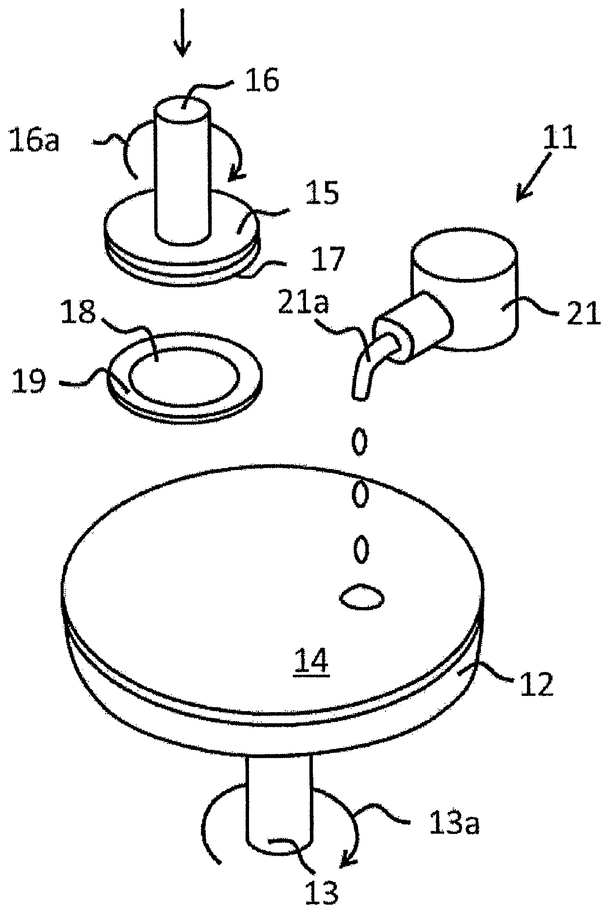
[0084]Using a polishing composition and a surface treatment composition each containing an abrasive (colloidal silica), a water-soluble polymer (hydroxyethyl cellulose: HEC, polyvinyl alcohol: PVA, polyacryloyl morpholine: PACMO), a surfactant (polyoxyethylene decyl ether: C10PEO5 only for an example 8, polyethyleneoxide-polypropyleneoxide-polyethyleneoxide: PEO-PPO-PEO only for an example 9), and a polishing composition and a surface treatment composition containing a basic compound (ammonia), which have kinds and contents illustrated in Table 1 respectively, a silicon wafer with a diameter of 300 mm was polish-treated and surface-treated and cleaned following it under the following conditions. Incidentally, in a comparative example 3, the surface treatment was performed under only pure water. In a comparative example 4, only a polishing step was substantially performed and completed.

[0085]Incidentally, the light scattering particle diameter of colloidal silica in Table is a volume...


PUM

PropertyMeasurementUnit
average primary particle diameteraaaaaaaaaa
temperatureaaaaaaaaaa

Abstract

There is provided a polishing method capable of more reducing defects on a silicon wafer surface. A polishing method of a silicon wafer, which includes a polishing step and a surface treatment step conducted after the polishing step and in which the number of abrasives in a surface treatment composition used in the surface treatment step is 1.0×10¹⁰ particles / mL or more and 1.0×10¹³ particles / mL or less by calculating from (1 [mL]×specific gravity of the composition [g / mL]×concentration of the abrasives [wt %]) / ((4 / 3)π×(average secondary particle diameter×10−7 [cm] / 2)3 [ / particle]×specific gravity of the abrasives [g / cm3]), using concentration of the abrasives in the surface treatment composition and an average secondary particle diameter measured by dynamic light scattering method, provided that all of the abrasives in the surface treatment composition used in the surface treatment step are assumed to have the average secondary particle diameter.

Description

CROSS REFERENCE TO RELATED APPLICATIONS[0001]This application is a continuation-in-part application of U.S. application Ser. No. 15 / 549,488, filed on Aug. 8, 2017, which is the National Stage of Application No. PCT / JP2016 / 000321 filed on Jan. 22, 2016, which is based upon and claims the benefit of priority from Japanese Application No. 2015-025350, filed Feb. 12, 2015 and Japanese Application No. 2015-087601, Filed Apr. 22, 2015, the entire contents of all of which are incorporated herein by reference.TECHNICAL FIELD[0002]The present invention relates to a polishing method of a silicon wafer, and particularly to a polishing method of a silicon wafer, including a surface treatment step conducted after a polishing step of the silicon wafer, and a surface treatment composition.BACKGROUND ART[0003]In order to realize high integration and high speed acceleration of an integrated circuit such as an ULSI or the like used in a computer, the fining of a design rule for a semiconductor device...

Claims


Application Information

Patent Timeline
Patent Type & Authority Patents(United States)
IPC IPC(8): H01L21/306B08B3/08B08B3/12C09G1/02B24B37/04H01L21/02
CPCH01L21/02052C09G1/02H01L21/02024B24B37/044B08B3/08B08B3/12H01L21/02057H01L21/30625
Inventor TSUCHIYA, KOHSUKE
Owner FUJIMI INCORPORATED
Features
  • R&D
  • Intellectual Property
  • Life Sciences
  • Materials
  • Tech Scout
  • Unparalleled Data Quality
  • Higher Quality Content
  • 60% Fewer Hallucinations
Learn More