Integrated coherent optical transceiver, light engine

a coherent optical transceiver and integrated technology, applied in the field of optical telecommunication techniques, can solve the problems of continuously demanding a huge amount of bandwidth for transferring photo, video, music, etc., and achieve the effects of improving communication bandwidth, increasing internet bandwidth, and rapid increase of serial link speed

Active Publication Date: 2020-08-25
MARVELL ASIA PTE LTD
View PDF4 Cites 41 Cited by
  • Summary
  • Abstract
  • Description
  • Claims
  • Application Information

AI Technical Summary

Benefits of technology

[0007]In modern electrical interconnect systems, high-speed serial links have replaced parallel data buses, and serial link speed is rapidly increasing due to the evolution of CMOS technology. Internet bandwidth doubles almost every two years following Moore's Law. But Moore's Law is coming to an end in the next decade. Standard CMOS silicon transistors will stop scaling around 5 nm. And the internet bandwidth increasing due to process scaling will plateau. But Internet and mobile applications continuously demand a huge amount of bandwidth for transferring photo, video, music, and other multimedia files. This disclosure describes techniques and methods to improve the communication bandwidth beyond Moore's law.
[0008]With the increase in the transmission capacity of WDM systems, coherent technologies attracted a renewal of widespread interest after 2000. The motivation is to develop methods for meeting the ever-increasing bandwidth demand with multi-level modulation formats based on coherent technologies. The first step in the revival of coherent optical communications research was triggered by quadrature phase-shift keying (QPSK) modulation / demodulation experiment featuring optical in-phase and quadrature (IQ) modulation (IQM) and optical delay detection. In such a scheme, we can double the bit rate while maintaining the symbol rate, and a 40-Gb / s differential QPSK (DQPSK) system has been put into practical use. Coherent transmitter has a transverse electric (TE) mode and transverse magnetic (TM) mode path. Silicon photonics chip operates essentially only in a TE only configuration. The signal has both TE mode and TM mode parts. To accomplish a silicon-photonics based integration of coherent transceiver, we need to have at least the following two components on the silicon photonics chip: 1) Polarization Beam Rotator Combiner (PBRC) integrated with a polarization-independent semiconductor optical amplifier (SOA) and driver in the coherent transmitter and 2) Polarization Beam Splitter Rotator (PBSR) integrated with electronics like transimpedance amplifier (TIA) in the coherent receiver, and to integrate the coherent transmitter and receiver with a tunable laser provided in a flip-chip.
[0009]In an embodiment, the present invention provides a tunable laser device based on silicon photonics. The tunable laser device includes a substrate configured with a patterned region comprising one or more vertical stoppers, an edge stopper facing a first direction, a first alignment feature structure formed in the patterned region along the first direction, and a bond pad disposed between the vertical stoppers. The tunable laser device further includes an integrated coupler built in the substrate located at the edge stopper. Additionally, the tunable laser device includes a laser diode chip including a gain region covered by a P-type electrode and a second alignment feature structure formed beyond the P-type electrode, the laser diode chip being flipped to rest against the one or more vertical stoppers with the P-type electrode attached to the bond pad and the gain region coupled to the integrated coupler. Furthermore, the tunable laser device includes a tuning filter fabricated in the substrate and coupled via a wire waveguide to the integrated coupler.

Problems solved by technology

But Internet and mobile applications continuously demand a huge amount of bandwidth for transferring photo, video, music, and other multimedia files.

Method used


Image

  • Integrated coherent optical transceiver, light engine
  • Integrated coherent optical transceiver, light engine
  • Integrated coherent optical transceiver, light engine

Examples


Embodiment Construction

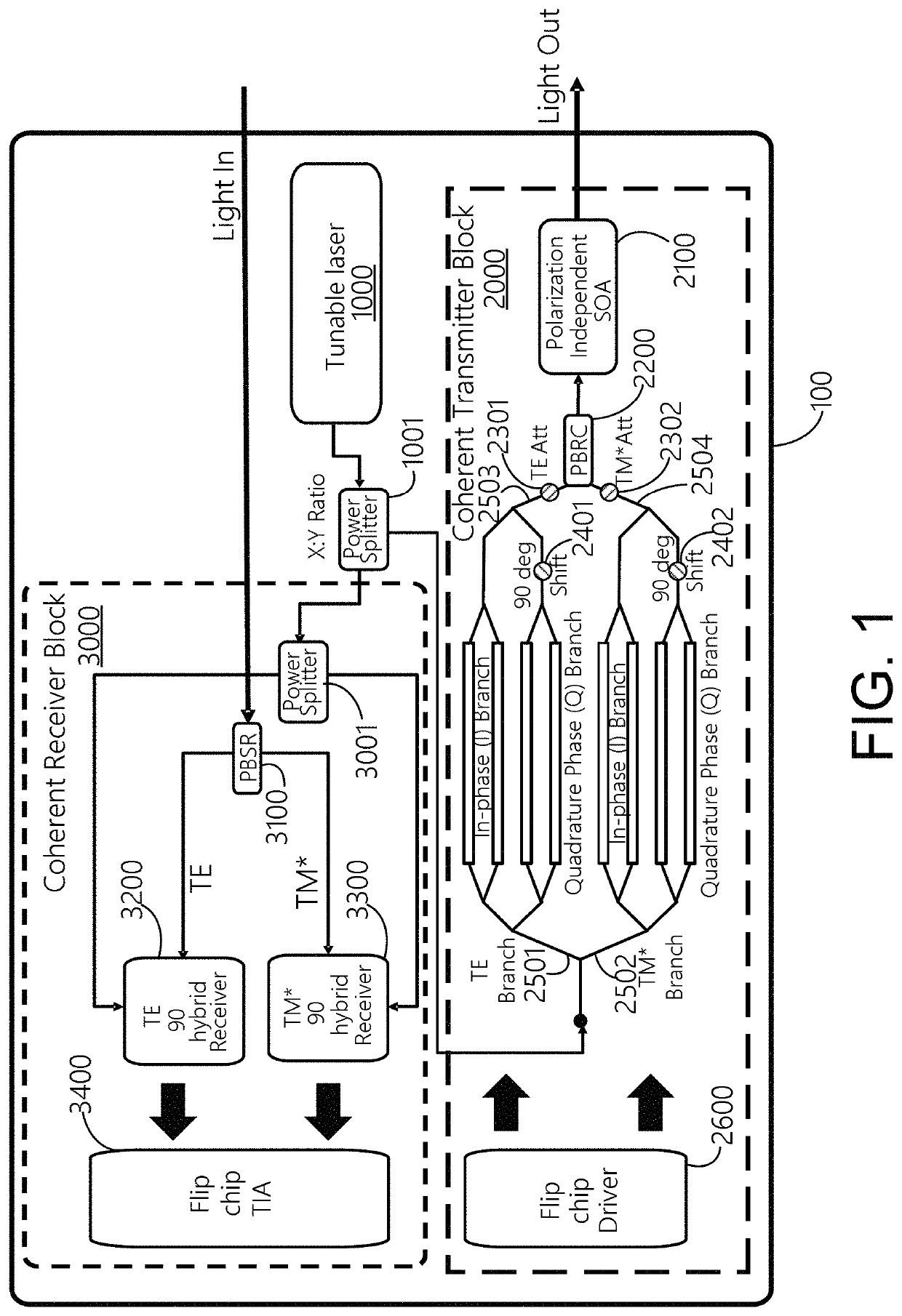
[0037]The present invention relates to optical telecommunication techniques. More particularly, the present invention provides an integrated compact coherent transceiver in silicon photonics platform. Merely by example, the present invention discloses a coherent transmitter block including a polarization independent semiconductor optical amplifier (SOA) coupled via polarization beam rotator combiner (PBRC) to a driver electronics chip and to an independently packaged wide-band tunable laser with silicon photonics tuning section, and a coherent receiver block including polarized hybrid receivers coupled to transimpedance amplifier (TIA) electronics chip via polarization beam splitter rotator (PBSR), and a method of integrating these components to form a coherent transceiver in a compact silicon photonics platform for wide-band DWDM optical communications, though other applications are possible.

[0038]The following description is presented to enable one of ordinary skill in the art to ...


PUM


Abstract

An coherent transceiver includes a single silicon photonics substrate configured to integrate a laser diode chip flip-mounted and coupled with a wavelength tuning section to provide a laser output with tuned wavelengths which is split in X:Y ratio partly into a coherent receiver block as local-oscillator signals and partly into a coherent transmitter block as a light source. The coherent receiver includes a polarization-beam-splitter-rotator to split a coherent input signal to a TE-mode signal and a TM*-mode signal respectively detected by two 90-deg hybrid receivers and a flip-mounted TIA chip assisted by two local-oscillator signals from the tunable laser device. The coherent transmitter includes a driver chip flip-mounted on the silicon photonics substrate to drive a pair of Mach-Zehnder modulators with 90-degree shift in quadrature-phase branches to modulate the laser output to two polarized signals with I/Q modulation and uses a polarization-beam-rotator-combiner to combine them as a coherent output signal.

Description

BACKGROUND OF THE INVENTION[0001]The present invention relates to optical telecommunication techniques. More particularly, the present invention provides a compact integrated coherent transceiver based on silicon photonics platform, a method for forming the same, and a system having the same.[0002]Over the last few decades, the use of communication networks exploded. In the early days Internet, popular applications were limited to emails, bulletin board, and mostly informational and text-based web page surfing, and the amount of data transferred was usually relatively small. Today, Internet and mobile applications demand a huge amount of bandwidth for transferring photo, video, music, and other multimedia files. For example, a social network like Facebook processes more than 500 TB of data daily. With such high demands on data and data transfer, existing data communication systems need to be improved to address these needs.[0003]40-Gbit / s and then 100-Gbit / s data rates wide-band DWD...

Claims


Application Information

Patent Timeline
Patent Type & Authority Patents(United States)
IPC IPC(8): G02B6/12H01S5/022H04B10/40H01S5/00G02B6/126G02B6/122G02B6/42H04J14/02H01S5/02375
CPCG02B6/1228G02B6/12004H01S5/0224G02B6/126G02B6/428G02B6/4246H04B10/40H01S5/0085G02B2006/12121G02B2006/12142G02B2006/12097G02B2006/12061G02B2006/12123H04J14/02H01S5/0262H01S5/06G02B6/4213G02B6/4296G02B6/4274H04B10/503H04B10/548H04B10/532H04B10/614H04B10/615H01S5/02375H01S5/021H01S5/142H01S5/1032H01S5/0687H01S5/4012G02B2006/1215G02B2006/12147H04B10/5053H01S5/0234H01S5/02326H01S3/13
Inventor NAGARAJAN, RADHAKRISHNAN L.
Owner MARVELL ASIA PTE LTD
Why Eureka
Try Eureka