Plasma etching method

a technology of etching method and plasma, which is applied in the fields of sustainable manufacturing/processing, greenhouse gas capture, climate sustainability, etc., can solve the problems of etching stop, etching is performed at the desired etching depth, and inhibit the etching rate, so as to reduce greenhouse gas emission, excellent etching characteristics, and low global warming potential

Active Publication Date: 2020-12-15
AJOU UNIV IND ACADEMIC COOP FOUND
View PDF6 Cites 0 Cited by
  • Summary
  • Abstract
  • Description
  • Claims
  • Application Information

AI Technical Summary

Benefits of technology

[0008]One purpose of the present disclosure is to provide a novel etchant which may replace the conventional PFC gas, have a low GWP and thus are environmentally friendly, have an excellent etching characteristic to allow a high aspect ratio etched structure to be formed, and is to provide a plasma etching method using the novel etchant.
[0015]In one implementation, the etching target includes silicon oxide, wherein a hole pattern mask is disposed on the etching target, wherein the plasma etching allows the etching target to have a high aspect ratio etched structure.
[0016]According to the plasma etching method according to the present disclosure, the etching target can be plasma-etched with excellent etching characteristics using the heptafluoropropyl methyl ether (HFE) gas with a very low global warming potential (GWP) of 530 which is much lower than that of the PFC gas. Therefore, in the plasma etching method using the HFE gas, the greenhouse gas emission can be reduced as compared with the semiconductor manufacturing process using the existing PFC gas, and thus, the plasma etching can be performed in an environmentally friendly manner. Further, according to the present invention, when performing the plasma etching using Ar and O2 gas together with the HFE gas, the etching target may be etched to achieve superior etching properties, and in particular, the deposition rate of the fluorocarbon film on the etching target is reduced while increasing the etching rate. Thus, the etching target can be etched while controlling a thickness of the carbon fluoride thin film in an appropriate manner. As a result, when the etching target is subjected to the plasma etching using a hole pattern mask, a high aspect ratio etched structure having little or no difference between a hole dimeter of the hole pattern mask and a diameter of the etched structure.

Problems solved by technology

However, the fluorocarbon thin film deposited at the time of plasma etching may inhibit the diffusion of reactive ions and radicals depending on the thickness, thereby inhibiting the etching rate.
Further, excessive deposition thereof on a wall of the etched structure causes etch stop, etc.
Thus, there is a problem that not only the etching is performed at a desired etching depth but also a diameter of a bottom of the etched structure is smaller than a hole diameter of the mask.
As a proportion of the etching process in the semiconductor device manufacturing processes increases, an annual amount of PFC gas emissions continues to increase.
However, those methods have fundamental limits due to the PFC gas having the high GWP.

Method used


Image

  • Plasma etching method
  • Plasma etching method
  • Plasma etching method

Examples


Embodiment Construction

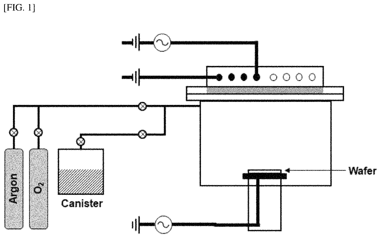
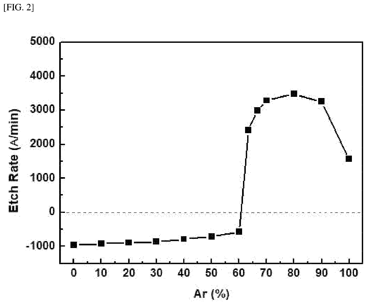
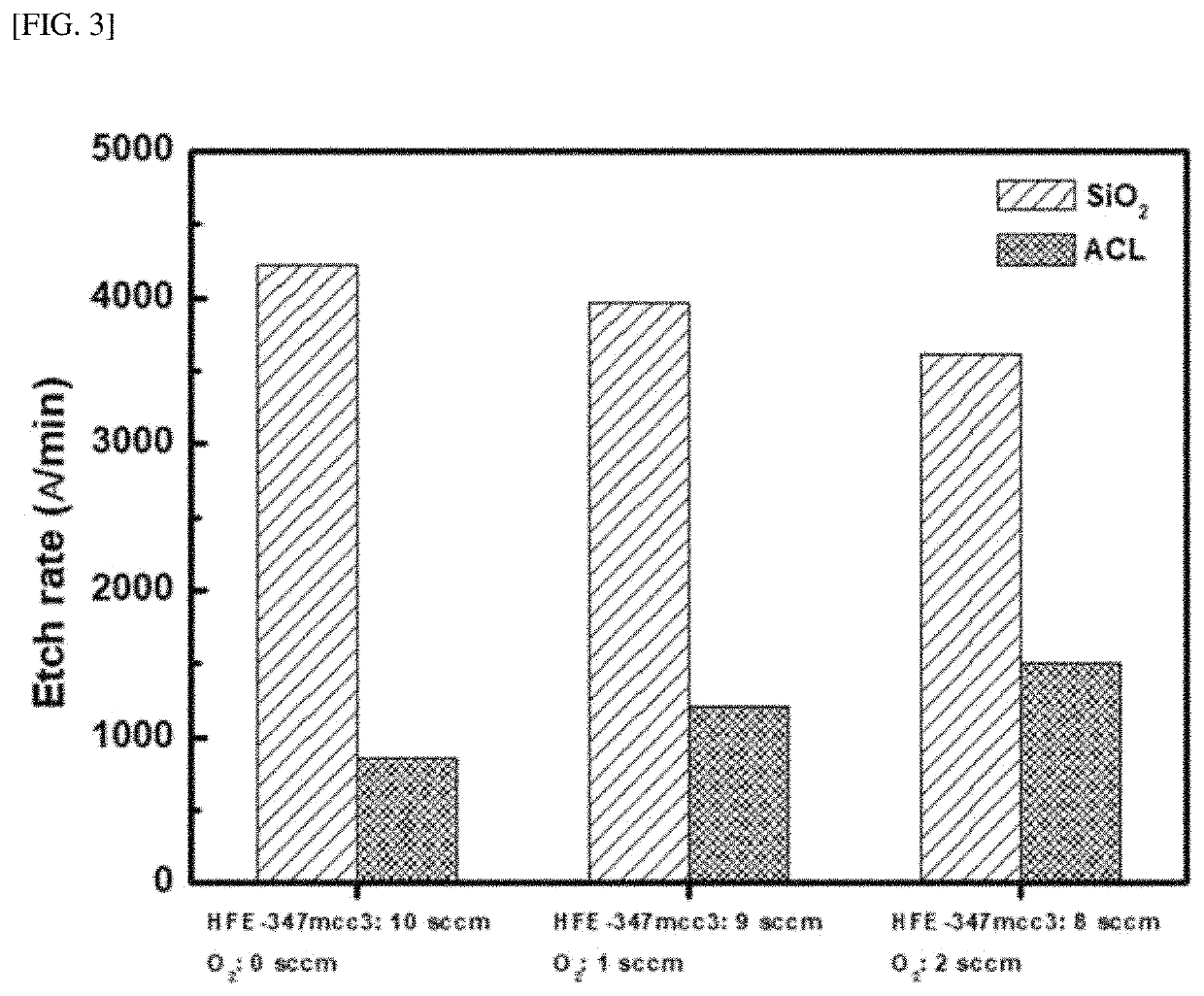
[0024]For simplicity and clarity of illustration, elements in the figures are not necessarily drawn to scale. The same reference numbers in different figures denote the same or similar elements, and as such perform similar functionality. Further, descriptions and details of well-known steps and elements are omitted for simplicity of the description. Furthermore, in the following detailed description of the present disclosure, numerous specific details are set forth in order to provide a thorough understanding of the present disclosure. However, it will be understood that the present disclosure may be practiced without these specific details. In other instances, well-known methods, procedures, components, and circuits have not been described in detail so as not to unnecessarily obscure aspects of the present disclosure.

[0025]Examples of various embodiments are illustrated and described further below. It will be understood that the description herein is not intended to limit the claim...


PUM

PropertyMeasurementUnit
GWPaaaaaaaaaa
boiling pointaaaaaaaaaa
bias voltageaaaaaaaaaa

Abstract

Provided is a plasma etching method comprising supplying heptafluoropropyl methyl ether (HFE) gas, argon (Ar) gas and oxygen (O2) gas to a plasma chamber receiving an etching target therein, thereby to plasma-etch the etching target.

Description

CROSS-REFERENCE TO RELATED APPLICATION[0001]This application claims a benefit under 35 U.S.C. § 119(a) of Korean Patent Application No. 10-2018-0094281 filed on Aug. 13, 2018, on the Korean Intellectual Property Office, the entire disclosure of which is incorporated herein by reference for all purposes.BACKGROUND1. Field[0002]The present disclosure relates to a plasma etching method using an etchant with a low global warming potential.2. Description of Related Art[0003]There is an increasing demand for a structure having a high aspect ratio due to high density of integrated circuits and miniaturization of devices in semiconductor devices. Generally, the high aspect ratio structure is fabricated in an insulating layer for electrically separating conductive layers from each other. Plasma etching of silicon oxide (SiO2) is widely used to manufacture such a high aspect ratio structure. Currently, perfluorocarbon (PFC) gas such as CF4, C2F6, C3F6, C3F8 and C4F8 is used in the plasma etch...

Claims


Application Information

Patent Timeline
Patent Type & Authority Patents(United States)
IPC IPC(8): C09K13/00H01L21/67H01L21/311C09G1/02
CPCH01L21/31116H01L21/31144C09G1/02C09K13/00H01L21/67069Y02C20/30Y02P70/50H01L21/3065H01L21/32136
Inventor KIM, CHANG-KOOKIM, JUN-HYUNPARK, JIN-SU
Owner AJOU UNIV IND ACADEMIC COOP FOUND
Why Eureka
Try Eureka