Method and system for co-packaging photonics integrated circuit with an application specific integrated circuit

a photonics and integrated circuit technology, applied in the field of co-packaging photonics integrated circuits with application specific integrated circuits, can solve the problems of limiting the aggregate bandwidth flowing through network switches, increasing the signaling rate dramatically, and increasing the loss of pcb trace loss

Active Publication Date: 2020-12-15
GHIASI ALI
View PDF4 Cites 8 Cited by
  • Summary
  • Abstract
  • Description
  • Claims
  • Application Information

AI Technical Summary

Benefits of technology

[0017]A system and / or method of assembling application specific integrated circuits (ASIC) dies on an inverted package substrate assembly with optoelectronic devices and Photonics Integrated Circuits (PIC) as shown in and / or described in connection with at least one of the figures and sets forth more completely in the claims.

Problems solved by technology

With the ever increasing of the network speed the conventional pluggable optics modules may limit the aggregate bandwidth flowing through network switches.
Increasing signaling rate or the use of higher order modulations are some of the options to improve bandwidth bottleneck between ASIC and pluggable optics modules but increasing the signaling rate will dramatically increase PCB trace loss and higher order modulations requires more complex digital signal processing (DSP) with significant added power.
Optics co-packaged with an application specific integrated circuits (ASIC) is viewed as the ultimate solution to eliminate copper interconnect (PCB or copper cable) bottlenecks between multi-Terabit ASIC and pluggable optics modules, but prior embodiments have not addressed manufacturability, serviceability, or thermal issues.
With ever increasing signaling rate copper interconnect that carries the data between the ASIC and pluggable optics module is becoming a bottleneck.

Method used


Image

  • Method and system for co-packaging photonics integrated circuit with an application specific integrated circuit
  • Method and system for co-packaging photonics integrated circuit with an application specific integrated circuit
  • Method and system for co-packaging photonics integrated circuit with an application specific integrated circuit

Examples


Embodiment Construction

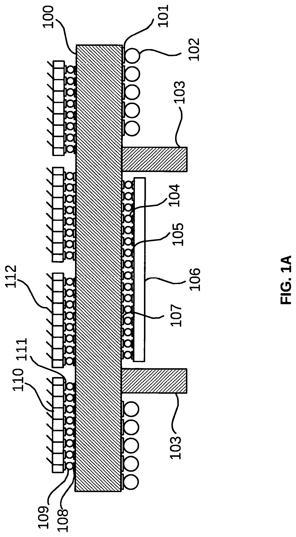
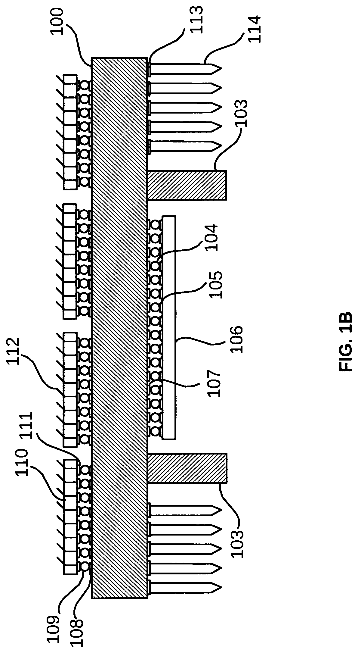
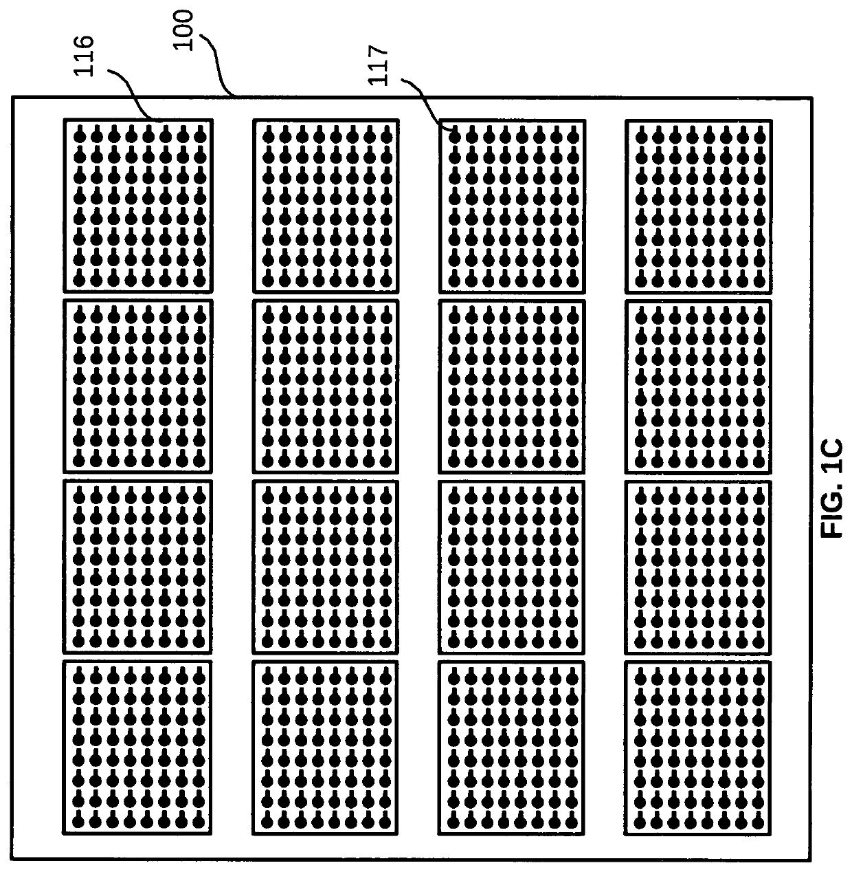
[0031]Present embodiment enhances application specific integrated circuits (ASIC) packages to allow assembly and co-packaging optoelectronics or photonic integrated circuits (PIC). Certain aspects of the disclosure may be found in the method and system of chip-scale and chiplet assembly. This embodiment supports high power ASICs, field programable gate arrays (FPGAs), graphic processor units (GPUs), or processors co-packaged with thermally sensitive optoelectronics components or PICs. The embodiment allows co-packaging high power ASIC devices with thermally sensitive optoelectronics PICs by mounting the ASIC on the bottom of the substrate on the same side as ball grid array (BGA) or pin grid array (PGA) contacts and mounting optoelectronics components or PICs on the substrate top surface and thermally isolating them from heat generated by the ASIC. By mounting the ASIC on the same side as the package BGA or PGA contacts, the full top surface of the package assembly is available to m...


PUM

PropertyMeasurementUnit
thermal isolationaaaaaaaaaa
rigidityaaaaaaaaaa
densityaaaaaaaaaa

Abstract

A method and system of co-packaging optoelectronics components or photonic integrated circuit (PIC) with application specific integrated circuits (ASICs) are disclosed and may include package substrate, several electronics die, passive components, socket assembly, and heat sinks. The said method converts ASIC high speed signals to optical signals by eliminating intermediary electrical interface between the ASIC and conventional optical modules. The method described provides many advantages of pluggable optical modules such as configurability, serviceability, and thermal isolation from the ASIC heat, while eliminating bandwidth bottlenecks as result of the ASIC package, host or linecard printed circuit board (PCB) traces, and the optical module connector. The high-power consumption ASIC is mounted below the package substrate, but sensitive optoelectronics and PIC components are mounted on top of the package substrate assembly for thermal isolation and serviceability. The package assembly ball grid array (BGA) or pin grid array (PGA) contacts are on the same side of the package substrate surface as ASIC die. The co-packaged package assembly is attached to the host or linecard PCB having a cutout for ASIC with the heatsink mounted from the bottom onto the ASIC die.

Description

CROSS-REFERENCE TO RELATED APPLICATIONS[0001]Not applicable.STATEMENT REGARDING FEDERALLY SPONSORED RESEARCH OR DEVELOPMENT[0002]Not applicable.THE NAMES OF THE PARTIES TO A JOINT RESEARCH AGREEMENT[0003]Not applicable.STATEMENT REGARDING PRIOR DISCLOSURES BY THE INVENTOR OR A JOINT INVENTOR[0004]Not applicable.BACKGROUND OF THE INVENTIONField of the Invention[0005]Int. Cl.[0006]G02B 6 / 13 (2018 November)[0007]G02B 6 / 43 (2018 November)[0008]G02B 6 / 43 (2018 November)[0009]H01S 5 / 024 (2018 November)[0010]U.S. Cl.[0011]CPC . . . G02B 6 / 428 (2019 May); G02B 6 / 4284 (2019 May); G02B 6 / 4269 (2019 May); G02B 6 / 43 (2019 May); G02B 6 / 13 (2019 May); H01S 5 / 024 (2019 May); H01S / 524 (2019 May); H04B 10 / 801 (2019 May)Description of Related Art[0012]The following is a tabulation of some prior arts that presently appears relevant:[0013]U.S. Pat.Pat. No.Kind CodeIssue DatePatentee 7,344,383B1Mar. 18, 2008Daoqiang Lu10,242,979B2Mar. 26, 2019Myung Jin Yim 9,910,232B2Mar. 6, 2018Attila Mekis 9,297,971B2...

Claims


Application Information

Patent Timeline
Patent Type & Authority Patents(United States)
IPC IPC(8): G02B6/42G02B6/43H01L23/00H04B10/40H04B10/25H04B10/516
CPCG02B6/425G02B6/4284G02B6/4272H01L24/17G02B6/43H01L24/13H01L24/16H04B10/40G02B6/4246H01L24/04G02B6/4292H01L24/14H04B10/25H01L2224/0401H01L2224/16227H01L2224/1703H01L2224/1403H04B10/516G02B6/4269G02B6/4274H01L23/36H01L23/49811H01L23/49816H01L23/5385H01L25/167H01L2224/13147H01L2924/15311H01L2924/15313H01L2924/15321H01L2924/15322H01L2924/00014
Inventor GHIASI, ALI
Owner GHIASI ALI
Why Eureka
Try Eureka