
Neuromorphic devices and circuits

a neuromorphic device and circuit technology, applied in pulse generators, pulse techniques, instruments, etc., can solve the problems of large increase in power consumption, large increase in area, and very serious heat release problems

Active Publication Date: 2020-12-15
SEOUL NAT UNIV R&DB FOUND
View PDF12 Cites 0 Cited by
  • Summary
  • Abstract
  • Description
  • Claims
  • Application Information

AI Technical Summary

Benefits of technology

The invention is a neuromorphic device and circuit that has improved reliability, low power consumption, and high integration. It solves problems of large area and high power consumption in previous neuron circuits. A neuron element with a memory function is utilized to greatly reduce the area of the circuit. Furthermore, the neuron element allows for uniform carrier concentration and reduces the number of elements needed. The device also introduces a function of storing charges in the gate electrodes, which can imitate various functions of a neuron.

Problems solved by technology

In recent years, in integrated circuits (von-Neumann-based integrated circuits) based on the Von Neumann architecture, power consumption has been greatly increased and the problem of heat release has been very serious.
Accordingly, the CMOS-based neuron circuits in the related art have the problems in that, due to a large size of the integrate capacitor, the entire area is greatly increased, and due to an increase in the number of elements, the area is increase, and the power consumption is also increased.
Due to these structural limitations, there are problem in that the configuration of the neuromorphic system is complicated, and there is a limitation in terms of accuracy.

Method used


Image

  • Neuromorphic devices and circuits
  • Neuromorphic devices and circuits
  • Neuromorphic devices and circuits

Examples


Embodiment Construction

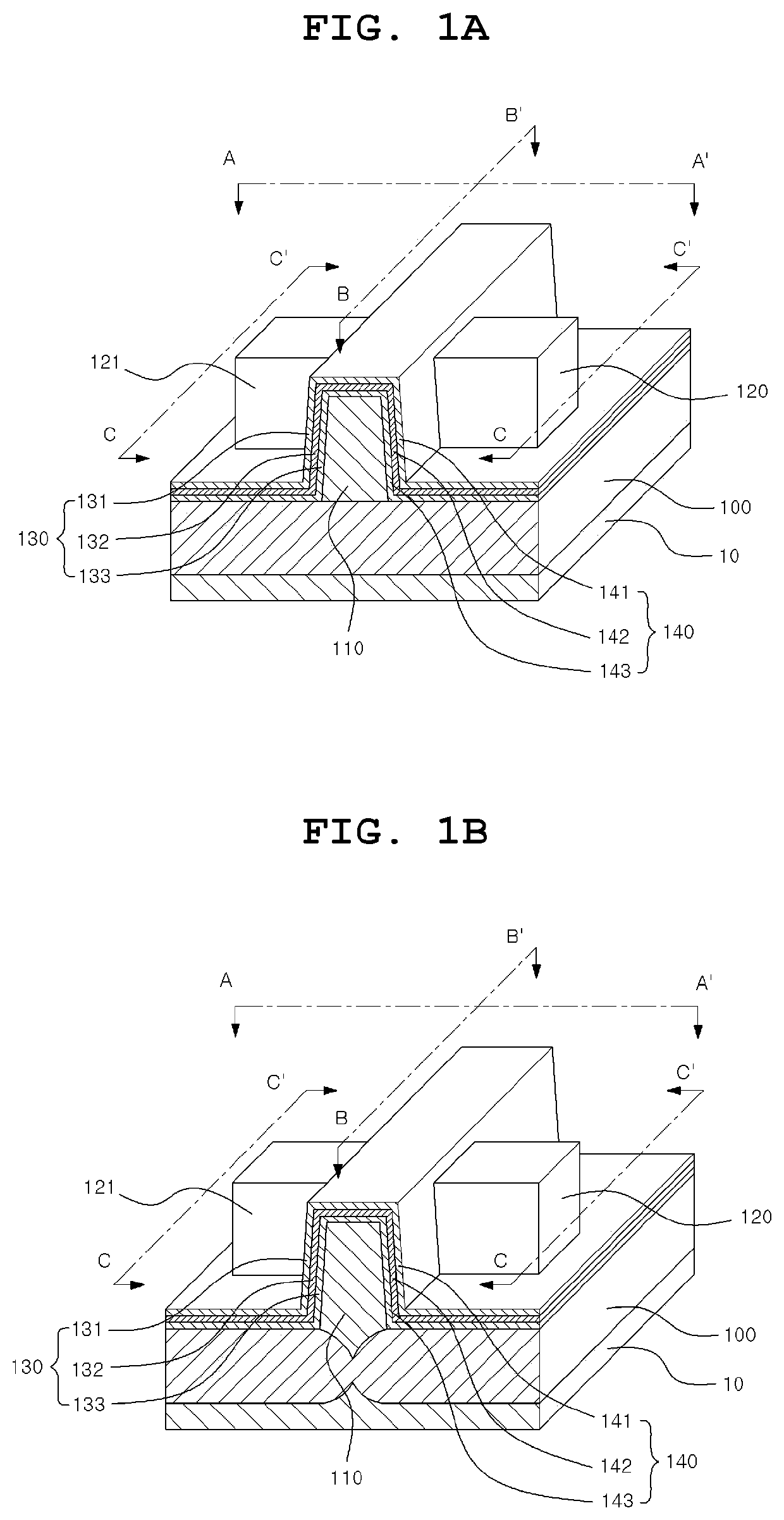
[0049]The invention provides a neuromorphic device and a neuromorphic circuit capable of being effectively integrated with a synapse array and having a low power and a high degree of integration. In particular, since the neuromorphic device according to the invention has an integrate function of a general neuron according to a program or erase operation in a charge storage layer, a neuromorphic system can be configured very effectively in terms of area. In addition, the neuromorphic device according to the invention not only has an integrate function but also performs a positive feedback operation of electrons and holes in a neuromorphic device when a certain threshold value is reached and instantaneously transmits a signal to the next synapse to be implemented in a small area.

[0050]Conceptually, the neuromorphic device according to the invention is a vertically configured wall-shaped thin semiconductor material or a horizontally thinned semiconductor material, which is separated fr...


PUM

PropertyMeasurementUnit
semiconductoraaaaaaaaaa
distanceaaaaaaaaaa
charge storageaaaaaaaaaa

Abstract

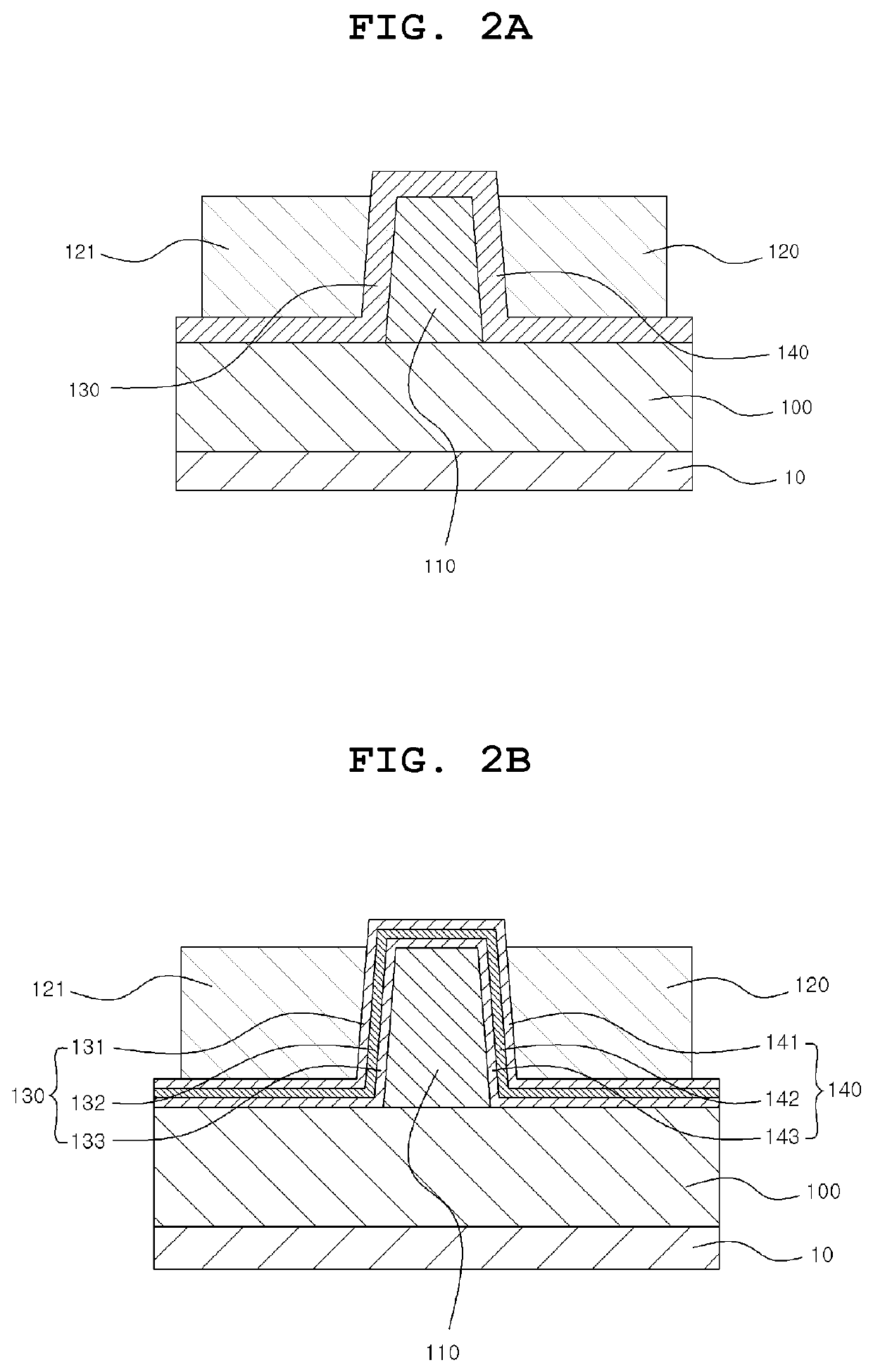
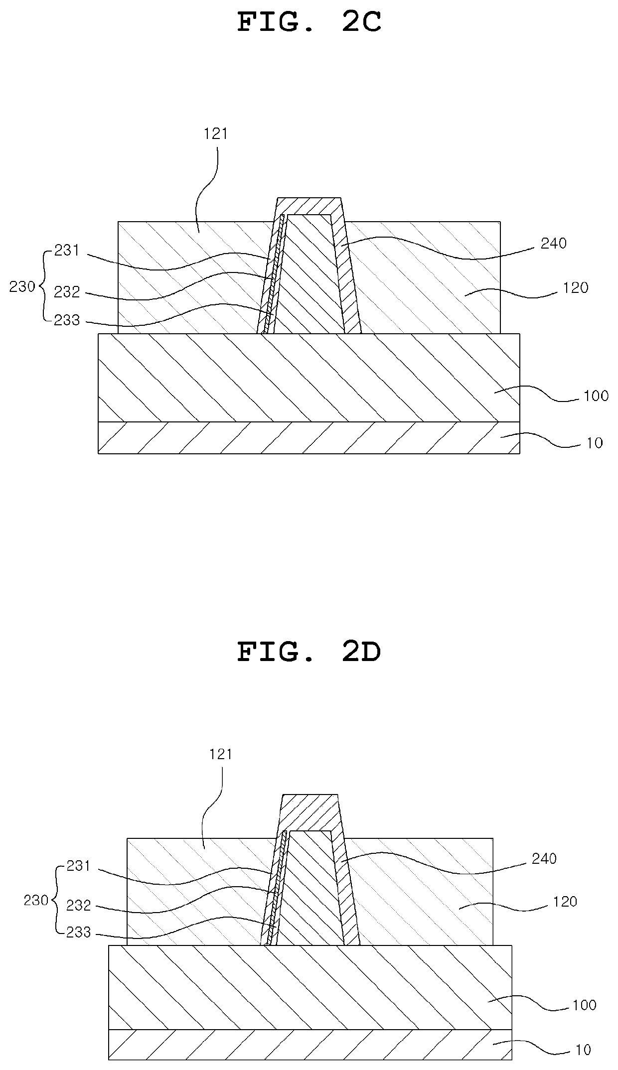
Provided are a neuromorphic device and a neuromorphic circuit using the neuromorphic device. The neuromorphic device is configured to include a first semiconductor region formed on a substrate in a wall shape or a dumbbell shape; first, second, third, and fourth doped regions sequentially formed in the first semiconductor region; first and second gate insulating film stacks disposed on the respective side surfaces of the second doped region; first and second gate electrodes respectively disposed on the respective side surfaces of the second doped region; the first and second gate electrodes disposed on the respective side surface of the second doped region, the first and second gate electrodes being electrically insulated from the second doped, region by the first and second gate insulating film stacks; and first and second electrodes electrically connected to the first and fourth doped regions, respectively.

Description

BACKGROUND OF THE INVENTION1. Field of the Invention[0001]The present invention relates to a neuromorphic device in a technique capable of imitating a neuron with a low power and a high degree of integration in a neuromorphic technique.2. Description of the Prior Art[0002]In recent years, in integrated circuits (von-Neumann-based integrated circuits) based on the Von Neumann architecture, power consumption has been greatly increased and the problem of heat release has been very serious. Therefore, many approaches to imitate nervous systems of animals have been studied. In particular, in techniques of imitating the nervous systems of animals the power consumption can be greatly reduced, and a cognitive function and learning are enabled, so that the cognitive function and s determination function can be improved.[0003]Accordingly, there is art opportunity to replace or greatly improve the functions of the existing von-Neumann-based integrated circuits. Therefore, much attention has be...

Claims


Application Information

Patent Timeline
Patent Type & Authority Patents(United States)
IPC IPC(8): H01L29/749H01L29/66H01L21/28G06N3/04G06N3/063H01L29/423H01L29/51H01L29/74H01L29/792H03K3/012H01L27/102H01L29/78
CPCH01L29/7436H01L29/513G06N3/049H03K3/012G06N3/0635H01L29/749H01L29/792H01L29/42308G06N3/0445H01L29/66833H01L29/42344H01L27/1027H01L29/40117H01L29/7855G06N3/065H10B69/00G06N3/063G06N3/04G06N3/044
Inventor LEE, JONG-HOWOO, SUNG YUN
Owner SEOUL NAT UNIV R&DB FOUND
Learn More