Semiconductor device and method for manufacturing the same

a semiconductor device and semiconductor technology, applied in the field of integrated circuits, can solve problems such as the difficulty of overcoming the soi mosfet device, and achieve the effect of significantly reducing the charging effect of the semiconductor devi

Active Publication Date: 2021-01-26
UNITED MICROELECTRONICS CORP
View PDF13 Cites 0 Cited by
  • Summary
  • Abstract
  • Description
  • Claims
  • Application Information

AI Technical Summary

Benefits of technology

[0005]The embodiments of the invention provide a semiconductor device in which a silicide layer is disposed between a backside contact and a backside interconnect structure, which solves the issue of metal loss of the backside contact and significantly reduces the charging effect of the semiconductor device.
[0006]The embodiments of the invention provide a method for manufacturing a semiconductor device that can simplify the manufacturing process and reduce the cycle time, which further enhances commercial competitiveness of the semiconductor device.
[0027]In light of the above, in the embodiments of the invention, the silicide layer is formed between the first contact and the second interconnect structure to solve the issue of metal loss of the first contact. Moreover, the silicide layers are respectively disposed between the first contact and the second interconnect structure and between the third contact and the second interconnect structure to discharge the charge accumulated in the first interconnect structure, which significantly reduces the charging effect of the semiconductor device. In addition, the method for manufacturing the semiconductor device of the embodiments of the invention can simplify the manufacturing process and reduce the cycle time, which further enhances commercial competitiveness of the semiconductor device.

Problems solved by technology

As the demand for high-performance circuits increases, the semiconductor-on-insulator (SOI) technique has attracted much attention because the conventional bulk metal-oxide-semiconductor field-effect transistor (MOSFET) structure cannot overcome issues such as short-channel effects, parasitic capacitance, and current leakage.
However, there are still some challenges in the SOI MOSFET device to overcome.

Method used


Image

  • Semiconductor device and method for manufacturing the same
  • Semiconductor device and method for manufacturing the same
  • Semiconductor device and method for manufacturing the same

Examples


first embodiment

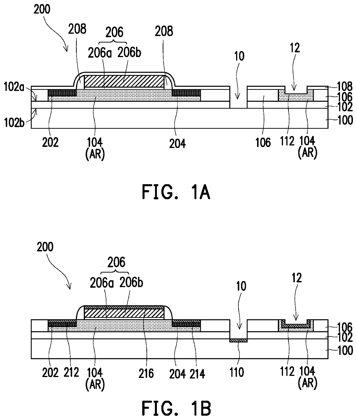
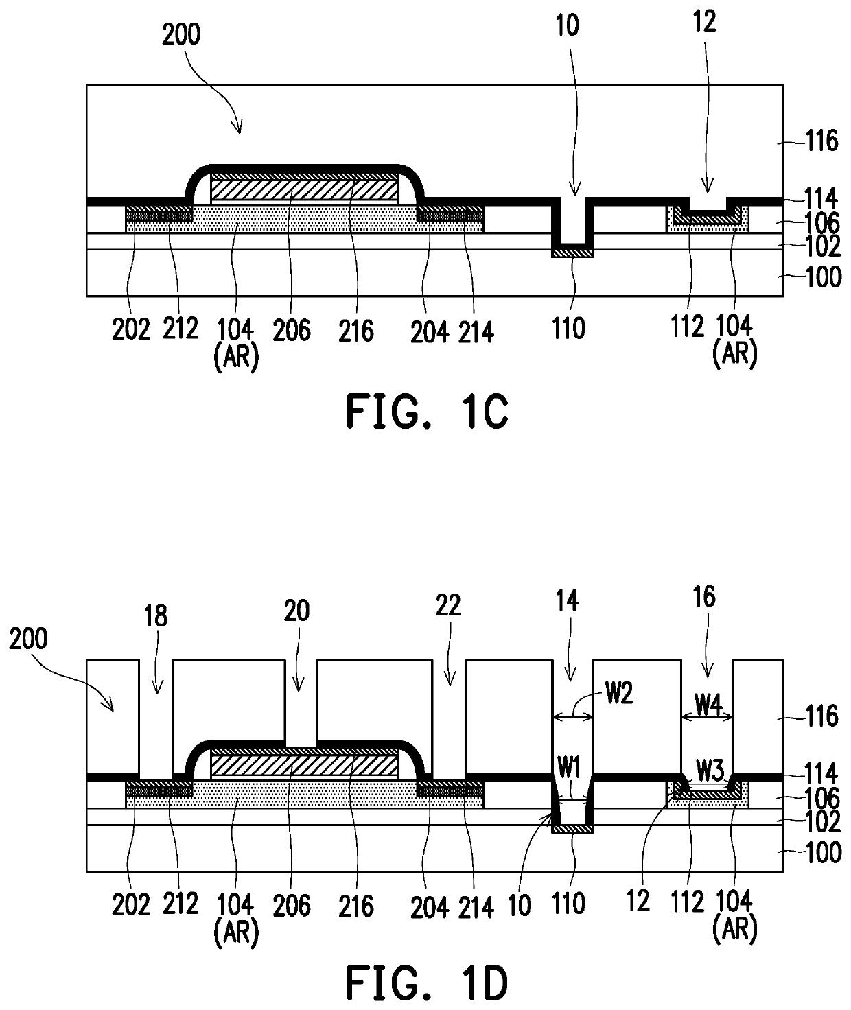
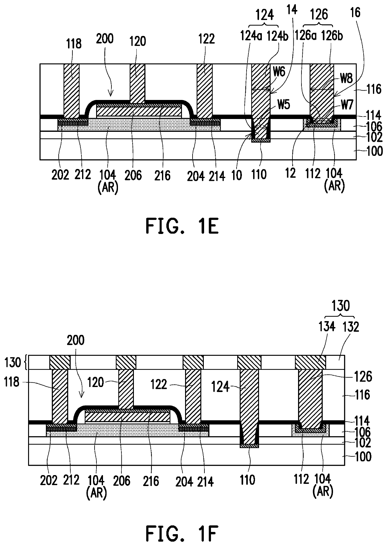
[0032]FIG. 1A to FIG. 1H are cross-sectional schematic diagrams illustrating a manufacturing process of a semiconductor device according to the invention. In the present embodiment, the semiconductor device may be a semiconductor device manufactured according to a radio frequency (RF) SOI technique, but the invention is not limited hereto.

[0033]Referring to FIG. 1A, a substrate 100 with an insulating layer 102 formed thereon is provided. The insulating layer 102 has a front side 102a and a back side 102b opposite to each other. The back side 102b of the insulating layer 102 is close to and in contact with the substrate 100. In an embodiment, the substrate 100 includes a semiconductor substrate, such as a silicon substrate. In an embodiment, a material of the insulating layer 102 includes an oxide, such as a silicon oxide layer. A thickness of the insulating layer 102 ranges from 500 Å to 1500 Å and is, for example, about 800 Å.

[0034]Next, a semiconductor layer 104 is formed on the f...

second embodiment

[0058]FIG. 2A to FIG. 2H are cross-sectional schematic diagrams illustrating a manufacturing process of a semiconductor device according to the invention.

[0059]Referring to FIG. 2A and FIG. 2H, basically, a method for manufacturing a semiconductor device 2 of the second embodiment is similar to the method for manufacturing the semiconductor device 1 of the first embodiment and shall not be repeatedly described here. The difference between the two lies in that when a second opening 14′ and a fourth opening 16′ are simultaneously formed in the interlayer dielectric layer 116 and the protective layer 114, as shown in FIG. 2D, a width W2′ of the second opening 14′ is greater than the width W1 of the first opening 10, and a width W4′ of the fourth opening 16′ is also greater than the width W3 of the recess 12. Therefore, when the protective layer 114 on the bottom surface of the first opening 10 and the protective layer 114 on the recess 12 are removed by using the silicide layers 110, 1...


PUM

PropertyMeasurementUnit
parasitic capacitanceaaaaaaaaaa
speedaaaaaaaaaa
packaging densityaaaaaaaaaa

Abstract

A semiconductor device and a method for manufacturing the semiconductor device are provided. The semiconductor device includes an insulating layer, a semiconductor layer, a plurality of isolation structures, a transistor, a first contact, a plurality of silicide layers, and a protective layer. The semiconductor layer is disposed on a front side of the insulating layer. The plurality of isolation structures are disposed in the semiconductor layer. The transistor is disposed on the semiconductor layer. The first contact is disposed beside the transistor and passes through one of the plurality of isolation structures and the insulating layer therebelow. The plurality of silicide layers are respectively disposed on a bottom surface of the first contact and disposed on a source, a drain, and a gate of the transistor. The protective layer is disposed between the first contact and the insulating layer.

Description

CROSS-REFERENCE TO RELATED APPLICATION[0001]This application claims the priority benefit of China application serial no. 201810466671.5, filed on May 16, 2018. The entirety of the above-mentioned patent application is hereby incorporated by reference herein and made a part of this specification.BACKGROUND OF THE INVENTIONField of the Invention[0002]The disclosure relates to an integrated circuit and a method for manufacturing the integrated circuit, and in particular, to a semiconductor device and a method for manufacturing the semiconductor device.Description of Related Art[0003]As the demand for high-performance circuits increases, the semiconductor-on-insulator (SOI) technique has attracted much attention because the conventional bulk metal-oxide-semiconductor field-effect transistor (MOSFET) structure cannot overcome issues such as short-channel effects, parasitic capacitance, and current leakage.[0004]In the SOI technique, a MOSFET device is formed on a semiconductor layer, and...

Claims


Application Information

Patent Timeline
Patent Type & Authority Patents(United States)
IPC IPC(8): H01L29/06H01L23/528H01L23/522H01L21/311H01L21/768H01L21/306H01L21/285
CPCH01L29/0649H01L21/30604H01L21/31111H01L21/76802H01L21/76831H01L21/76898H01L23/528H01L23/5226H01L21/28518H01L29/78H01L29/66568H01L23/5386H01L21/76895H01L21/76264H01L21/823475H01L27/088H01L21/84H01L27/1203H01L29/78639H01L29/78654H01L29/458
Inventor LI, WEN-SHENWEN, CHING-YANGVERMA, PURAKH RAJCHEN, XINGXINGNG, CHEE-HAU
Owner UNITED MICROELECTRONICS CORP
Why Eureka
Try Eureka