
Seal ring structure, semiconductor die, and method for detecting cracks on semiconductor die

a technology of sealing rings and semiconductor dies, applied in the field of semiconductor dies, can solve problems such as the importance of cracking

Active Publication Date: 2021-05-04
MEDIATEK INC
View PDF10 Cites 1 Cited by
  • Summary
  • Abstract
  • Description
  • Claims
  • Application Information

AI Technical Summary

Benefits of technology

The patent describes a method for detecting cracks on a semiconductor die. A seal ring is formed on the semiconductor substrate and includes two layers of interconnect elements. The resistance of the substrate between the interconnect elements is measured through the seal ring using a sensing circuit, which can determine if there is a crack present in the substrate. This technique allows for the detection of cracks during semiconductor device manufacturing, improving yield and reliability.

Problems solved by technology

However, the issue of cracking is still important due to the further scaling-down of the semiconductor device and increasing demands for smaller dimensions and more functions in consumer products.

Method used


Image

  • Seal ring structure, semiconductor die, and method for detecting cracks on semiconductor die
  • Seal ring structure, semiconductor die, and method for detecting cracks on semiconductor die
  • Seal ring structure, semiconductor die, and method for detecting cracks on semiconductor die

Examples


Embodiment Construction

[0016]The following description is of the best-contemplated mode of carrying out the invention. This description is made for the purpose of illustrating the general principles of the invention and should not be taken in a limiting sense. The scope of the invention is best determined by reference to the appended claims.

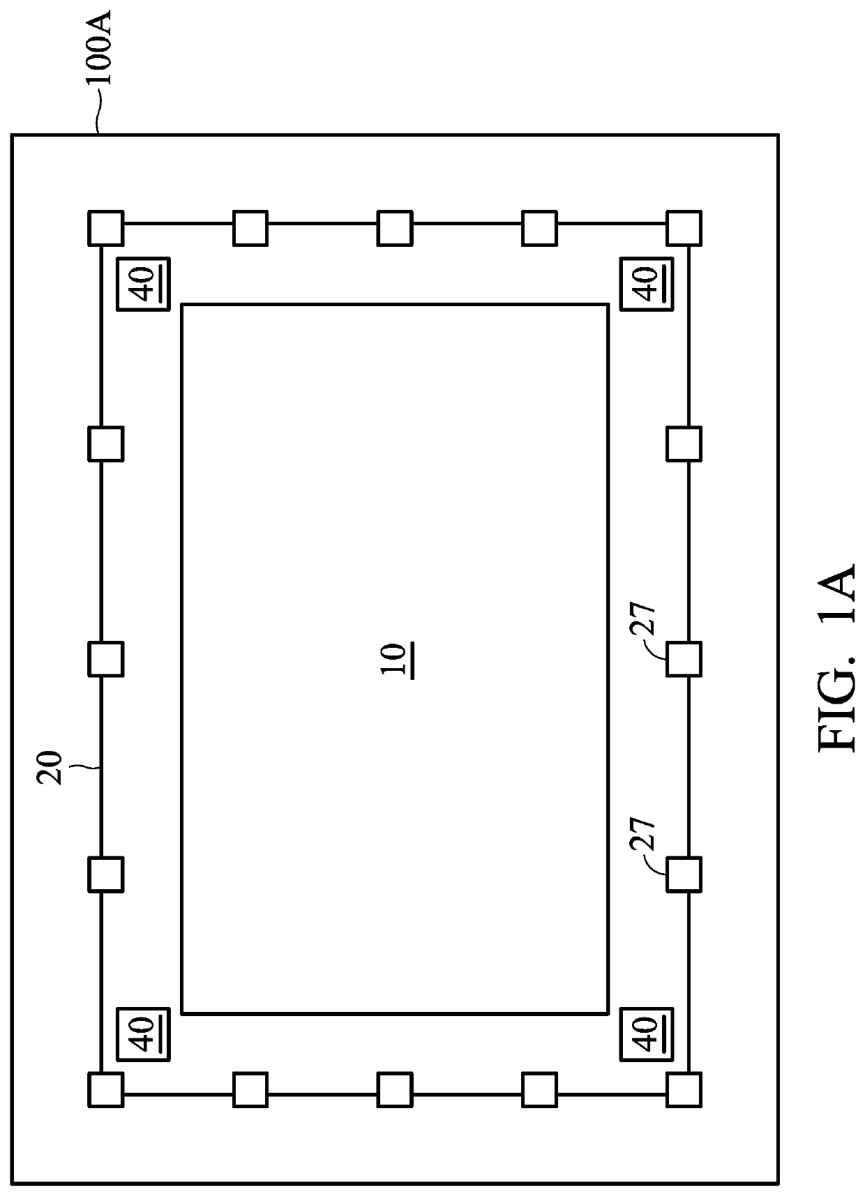
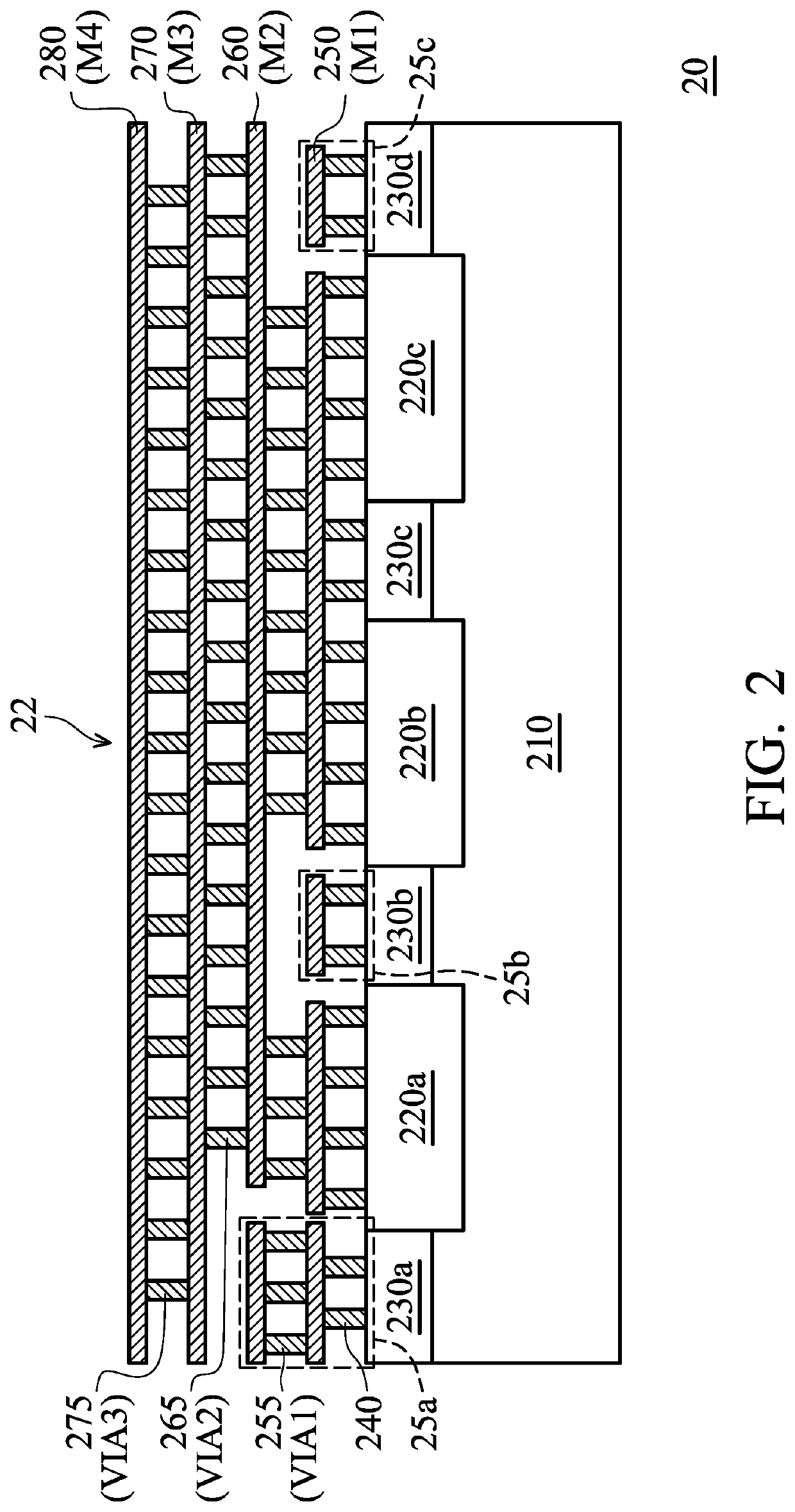
[0017]Die seal ring structures (also referred to as ‘chip seal rings’ or ‘seal rings’) are commonly used around the periphery of integrated circuits (ICs) in order to protect the circuit components from mechanical damage both during assembly and in operation. The main risk of mechanical damage in assembly arises from cracks in the dielectric layers which may occur when a processed wafer is diced into individual die (e.g. using a wafer saw). These cracks in the dielectric layers may then propagate further into the die if it is thermally cycled (e.g. during assembly or during operation). Other damage, such as chipping, may also occur when the wafer is diced. In operation...


PUM

PropertyMeasurementUnit
external stressaaaaaaaaaa
heightaaaaaaaaaa
semiconductoraaaaaaaaaa

Abstract

A seal ring structure is provided. The seal ring structure includes a seal ring on a semiconductor substrate. The seal ring includes a first interconnect element and a plurality of second interconnect elements. The first interconnect element is formed on a shallow trench isolation (STI) region and a first group of P-type doping regions over the semiconductor substrate. The second interconnect elements are formed below the first interconnect element and on a second group of P-type doping regions over the semiconductor substrate. The second interconnect elements are electrically separated from the first interconnect element, and the first and second groups of P-type doping regions are separated by the STI region.

Description

CROSS REFERENCE TO RELATED APPLICATIONS[0001]This Application claims priority of U.S. Provisional Application No. 62 / 592,532, filed on Nov. 30, 2017, the entirety of which is incorporated by reference herein.BACKGROUND OF THE INVENTIONField of the Invention[0002]The invention relates to a semiconductor die, and more particularly to a semiconductor die with a seal ring for detecting cracks.Description of the Related Art[0003]A seal ring is generally formed between scribe lines and integrated circuits of each die on a wafer, and the seal ring is formed by alternatively laminating dielectric layers and metal layers, which interconnect by vias through the dielectric layers. When a wafer dicing process is performed along the scribe lines, the seal ring can block unintended stress cracks from the scribe lines to the integrated circuits produced during the wafer dicing process. Also, the die seal ring can block moisture penetration or chemical damage like acid, alkaline containing or diffu...

Claims


Application Information

Patent Timeline
Patent Type & Authority Patents(United States)
IPC IPC(8): H01L23/00H01L21/66H01L21/765H01L29/40G01R31/28G01R27/02H01L23/522H01L23/58
CPCH01L23/562G01R27/02G01R31/2831H01L21/765H01L22/32H01L22/34H01L23/522H01L23/585H01L29/402H01L23/5226G01N27/041G01N27/20H01L23/564
Inventor PAN, CHUNG-WEFU, CHING-HUNGFAN, KUO-LUNG
Owner MEDIATEK INC
Learn More