TFT pixel threshold voltage compensation circuit with global compensation

Active Publication Date: 2021-05-18
SHARP KK
View PDF8 Cites 3 Cited by
  • Summary
  • Abstract
  • Description
  • Claims
  • Application Information

AI Technical Summary

Benefits of technology

The present invention relates to pixel circuits that can compensate for variations in the threshold voltage of the drive transistor with a very short horizontal time of less than about 2 μs. This is done by separating the threshold compensation and data programming phases, which allows for additional memory effects to be removed from the previous frame. To achieve this, a two-capacitor pixel circuit configuration is used, where the first capacitor is used for drive transistor threshold compensation and the second capacitor is used to store the data voltage during a data pre-loading phase. The use of an ultra-low leakage oxide transistor as the data switch device makes it possible to retain the stored data voltage for longer periods of time due to the ultra-low leakage. A conventional typical refresh rate of 60 Hz can be reduced to 30 Hz or lower for static images, which leads to lower power consumption. The use of a dual transistor configuration to reset circuit voltages for the current frame and save power during the initialization phase is also described in the present invention.

Problems solved by technology

The threshold compensation time is decided by the drive transistor characteristics and is difficult to reduce further without degrading the compensation accuracy.

Method used


Image

  • TFT pixel threshold voltage compensation circuit with global compensation
  • TFT pixel threshold voltage compensation circuit with global compensation
  • TFT pixel threshold voltage compensation circuit with global compensation

Examples


Embodiment Construction

"d_n">[0029]Embodiments of the present application will now be described with reference to the drawings, wherein like reference numerals are used to refer to like elements throughout. It will be understood that the figures are not necessarily to scale.

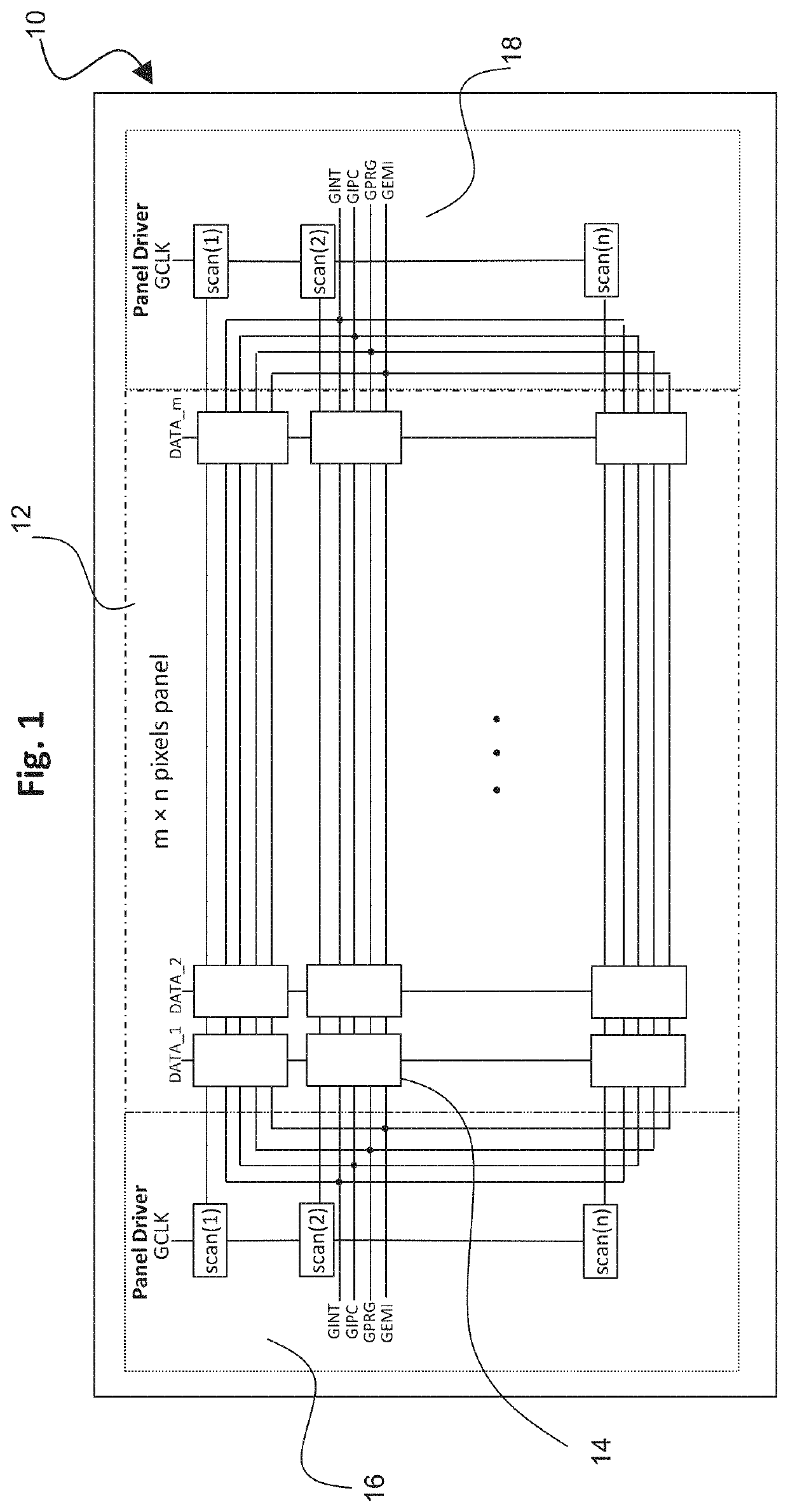
[0030]FIG. 1 is a drawing depicting a display panel configuration 10 in accordance with embodiments of the present application. The display panel 10 includes a pixel array 12 of “n” rows and “m” columns of individual pixels 14, and panel drivers 16 and 18 located respectively on the left and right edges of the display panel 10 on opposite sides of the pixel array 12. The panel drivers 16 and 18 operate comparably as each other in applying comparable control signals as further detailed below. Multiple panel drivers are used to prevent signal degradation across the display panel, and applying control signals from panel drivers on opposite sides of the pixel array 12 ensures effective control signals are received by the individual pixels ...


PUM


Abstract

A pixel circuit compensates the threshold voltage variations of the drive transistor with an ultra-short one horizontal (1H) time, with additionally removing the possible memory effects associated with the light-emitting device and the drive transistor from the previous frame. An ultra-short 1H time (<2 μs) is achieved via separation of threshold compensation of the drive transistor and data programming phases. The pixel circuit has a two-capacitor configuration, whereby a first capacitor is used for drive transistor threshold compensation, and a second capacitor is used to store the data voltage during a data pre-loading phase. Two transistors are employed to electrically connect the gate and source of the drive transistor to a common initialization voltage during an initialization phase to reset circuit voltages for the current frame. In this manner, no current flows through the drive transistor to the light-emitting device during the initialization phase when the light-emitting device does not emit light, which saves power. An array of individual pixel circuits is controlled using a global compensation scheme in which global control signals are applied to the individual pixel circuits of the pixel array.

Description

TECHNICAL FIELD[0001]The present invention relates to design and operation of electronic circuits for delivering electrical current to an element in a display device, such as for example to an organic light-emitting diode (OLED) in the pixel of an active matrix OLED (AMOLED) display device.BACKGROUND ART[0002]Organic light-emitting diodes (OLED) generate light by re-combination of electrons and holes, and emit light when a bias is applied between the anode and cathode such that an electrical current passes between them. The brightness of the light is related to the amount of the current. If there is no current, there will be no light emission, so OLED technology is a type of technology capable of absolute blacks and achieving almost “infinite” contrast ratio between pixels when used in display applications.[0003]Several approaches are taught in the prior art for pixel thin film transistor (TFT) circuits to deliver current to an element of a display device, such as for example an org...

Claims


Application Information

Patent Timeline
IPC IPC(8): G09G3/3258G09G3/3266G09G3/325G09G3/3283
CPCG09G3/325G09G3/3283G09G2310/0294G09G2320/0204G09G2320/0233G09G3/3225G09G3/3233G09G2300/0819G09G2300/0842G09G2300/0861G09G2310/0251G09G2330/021
Inventor LU, TONGBROWNLOW, MICHAEL JAMESSMEETON, TIM MICHAEL
Owner SHARP KK
Why Eureka
Try Eureka