Electrophotographic photosensitive member, process cartridge, and electrophotographic apparatus
a photosensitive member and electrophotography technology, applied in the direction of electrographic process apparatus, optics, instruments, etc., can solve the problems of reducing the hardness repulsion of the surface layer, and inferiority of organic materials to inorganic materials
- Summary
- Abstract
- Description
- Claims
- Application Information
AI Technical Summary
Benefits of technology
Problems solved by technology
Method used
Image

Examples
example 1
[0204]
[0205]
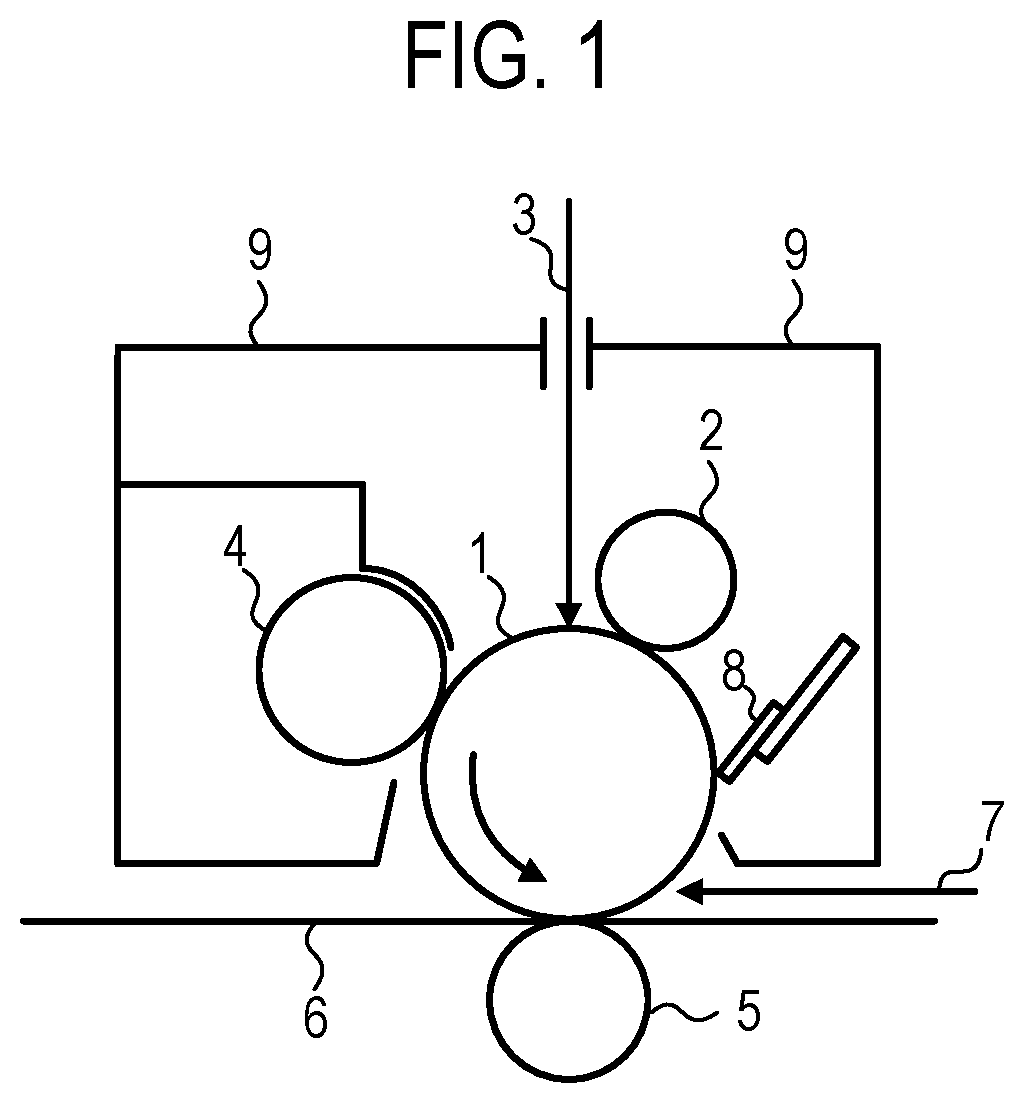
[0206]As a support, a cylindrical aluminum cylinder having a diameter of 29.9 mm, a length of 357.5 mm, and a thickness of 0.7 mm was used.
[0207]
[0208]As a metal oxide, 100 parts by mass of zinc oxide particles (specific surface area: 19 m2 / g, powder resistance: 4.7×10⁶ Ω·cm) were mixed with 500 parts by mass of toluene with stirring. To this mixture, 0.8 parts by mass of N-2-(aminoethyl)-3-aminopropylmethyldimethoxysilane (trade name: KBM602, manufactured by Shin-Etsu Chemical Co., Ltd.) was added as a silane coupling agent, and the mixture was stirred for 6 hours. Thereafter, toluene was distilled off under reduced pressure, and the residue was heat-dried at 140° C. for 6 hours to afford surface-treated zinc oxide particles.
[0209]Subsequently, 15 parts by mass of polyvinyl butyral (trade name: S-LEC (registered trademark) B BM-1, manufactured by SEKISUI CHEMICAL CO., LTD.) and 15 parts by mass of blocked isocyanate (trade name: Sumidur 3175, manufactured by Sumitomo Ba...
example 2
[0250]A compound represented by the formula (1-5) was used instead of the compound represented by the formula (1-1) in Example 1. An electrophotographic photosensitive member of Example 2 was prepared as in Example 1 except for the above-described modification.
examples 3 to 9
[0251]Types of compounds represented by the formula (1) and mass ratios among materials as shown in the following Table 1 were used instead of those in Example 1. Electrophotographic photosensitive members of Examples 3 to 9 were prepared as in Example 1 except for the above-described modifications.
[0252]In the following table, A, B, and C represent the mass of the curable hole-transport compound, the mass of the compound represented by the formula (1), and the mass of the compound represented by the formula (2), respectively.
[0253]
TABLE 1FilmCompoundthicknessrepresentedofbyA / (A +B / (A +C / (A +protectionformula (1)B + C)B + C)B + C)layer [μm]Example 31-10.7000.2000.1005Example 41-50.7000.1000.2005Example 51-50.7750.2000.0255Example 61-50.5000.1000.4005Example 71-50.7000.1500.1501Example 81-50.7000.1500.15010Example 91-50.7000.1500.1505
PUM
| Property | Measurement | Unit |
|---|---|---|
| thickness | aaaaa | aaaaa |
| thickness | aaaaa | aaaaa |
| wavenumber | aaaaa | aaaaa |
Abstract
Description
Claims
Application Information