Device and method for controlling switching

a technology of switching device and switch, applied in the direction of electronic switching, pulse technique, transistor, etc., can solve the problems of high switching speed, voltage overshoot between drains, affecting the performance of power semiconductor switch, etc., and achieve the effect of reducing ringing and low voltage overshoo

Active Publication Date: 2021-06-15
MITSUBISHI ELECTRIC CORP
View PDF6 Cites 0 Cited by
  • Summary
  • Abstract
  • Description
  • Claims
  • Application Information

AI Technical Summary

Benefits of technology

[0008]The present invention aims to allow a fast switching with a low voltage overshoot and reduced ringing at the end of the switching either during turn-on and turn-off using an active controlled feedback signal that is injected in the gate driver circuit.
[0018]Thus, the present invention reduces the current transient rate and / or the voltage overshoot.
[0022]Thus, the current sensor is controlling the semiconductor power switch only during transition avoiding any spurious shoot through during the rest of the switching period.

Problems solved by technology

High switching speed may create voltage overshoots between drain and source of power semiconductor transistor for example due to the layout stray inductance increasing the switching losses and over stressing the transistor.
However, this permanent modification on the gate driver circuit impacts the performance of the power semiconductor switch.

Method used


Image

  • Device and method for controlling switching
  • Device and method for controlling switching
  • Device and method for controlling switching

Examples


Embodiment Construction

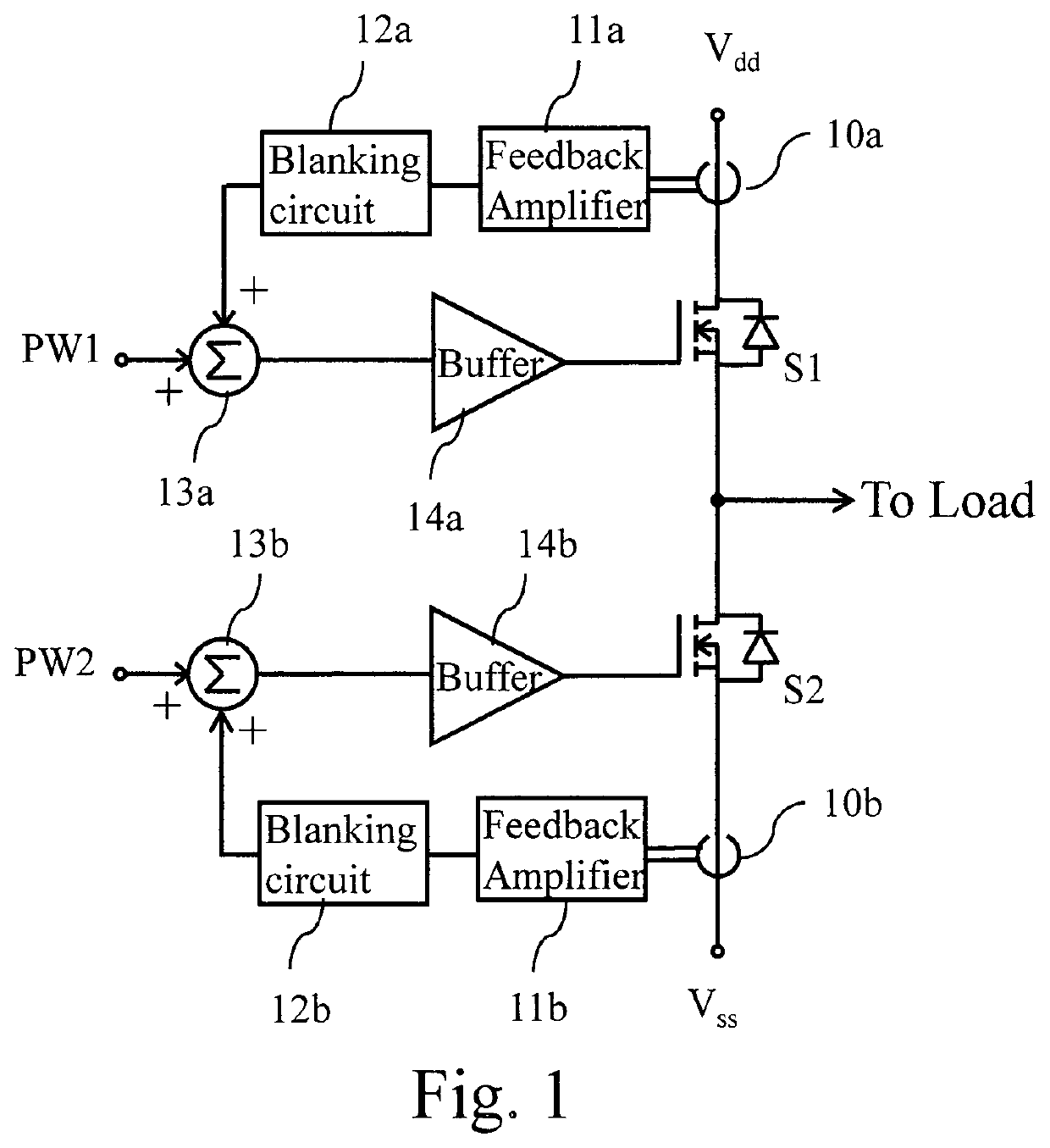
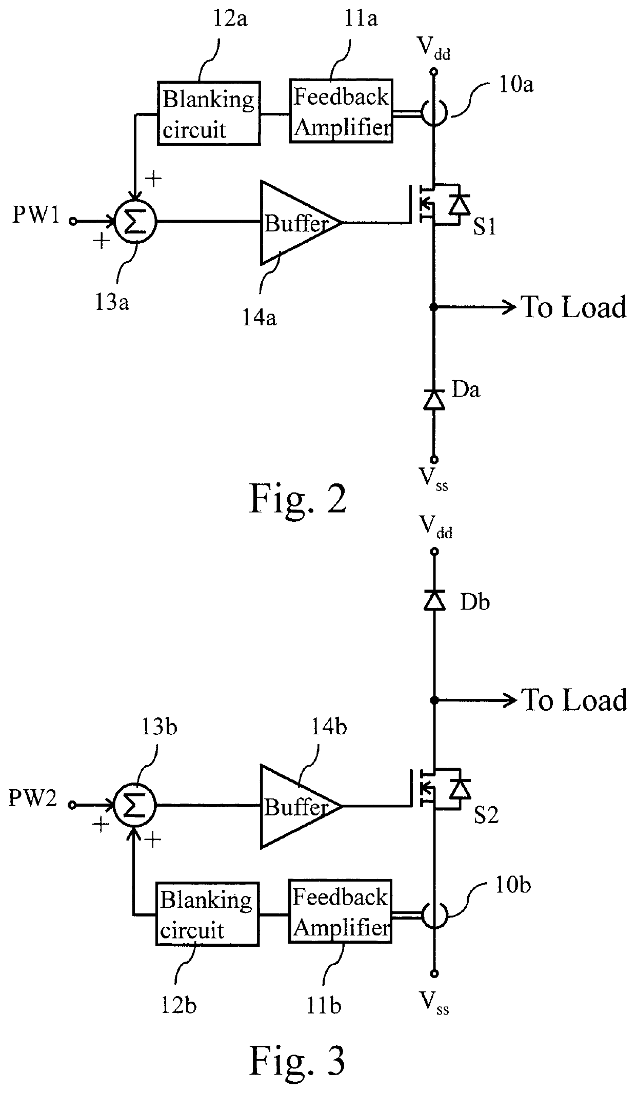
[0039]FIG. 1 represents an example of an architecture of a half bridge configuration in which the present invention may be implemented.

[0040]In the example of FIG. 1, a first gate trajectory control device which is composed of a current derivative sensing means 10a, a feedback amplifier 11a, a blanking circuit 12a, a summing circuit 13a and a buffer 14a, controls the switching of a power semiconductor switch S1 and a second gate trajectory control device which is composed of a current derivative sensing means 10b, a feedback amplifier 11b, a blanking circuit 12b, a summing circuit 13b and a buffer 14b, controls the switching of a power semiconductor switch S2.

[0041]The present invention is disclosed in an example based on an MOSFET application but can be extended to any unipolar (JFET, IGFET, HEMT) or bipolar transistor (BJT or IGBT), only the name of the electrodes needs to be changed.

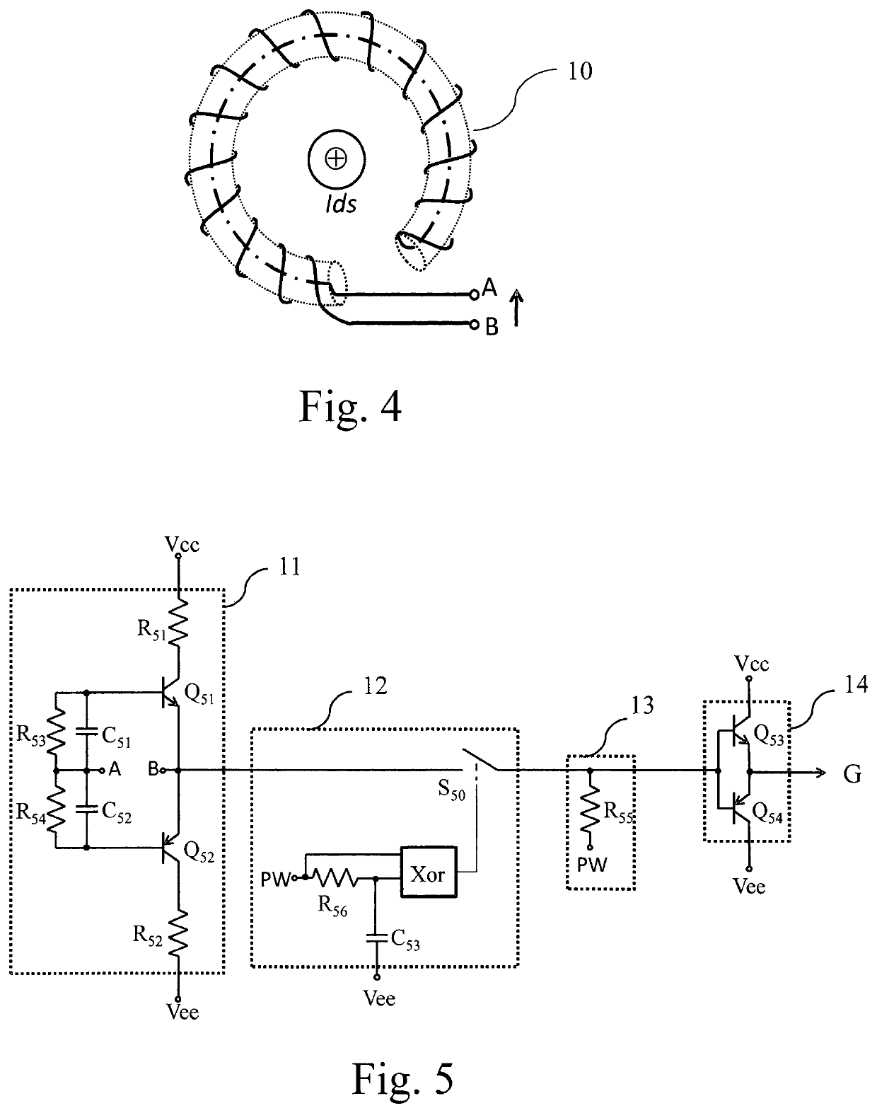
[0042]The present invention performs the switching of a power MOSFETs in two steps. At a first ste...


PUM

PropertyMeasurementUnit
currentaaaaaaaaaa
voltageaaaaaaaaaa
gate transition timeaaaaaaaaaa

Abstract

The present invention concerns a device and a method for controlling the switching from a conducting state to a non conducting state or from a non conducting state to a conducting state of a semiconductor power switch providing current to a load, the device receiving an input signal that is intended to drive the semiconductor power switch. The invention: —senses the derivative of the drain to source current going through the semiconductor power switch in order to obtain a voltage representative of the sensed derivative of drain to source current, —amplifies the voltage representative of the sensed derivative of drain to source current, —adds the amplified voltage representative of the derivative of the sensed drain to source current to the input signal during a given time period.

Description

TECHNICAL FIELD[0001]The present invention relates generally to a device and a method for controlling the switching of at least a first power semiconductor switch providing current to a load.BACKGROUND ART[0002]A classical gate driver circuit contains fixed positive and negative voltage / current power supplies called Vcc for the positive voltage and Vee for the negative one, both referenced to the source of the semiconductor switch. Depending on the desired state of the semiconductor switch, the power semiconductor switch gate is connected to either supply rail by means of a switch and an optional gate resistance. For turning-on the semiconductor switch, the positive voltage / current source is connected to the gate control of the semiconductor switch, for turning-off the semiconductor switch the negative voltage / current source is connected to the gate control of the device.[0003]Today, the switching frequency of power converters is increasing. Wide-band gap devices like GaN and SiC de...

Claims


Application Information

Patent Timeline
Patent Type & Authority Patents(United States)
IPC IPC(8): H03K17/042H02M1/08H03K17/16H02M1/00
CPCH03K17/04206H02M1/08H03K17/165H02M2001/0009H02M2001/0054H03K17/166Y02B70/10H02M1/0009H02M1/0054
Inventor MORAND, JULIENBRANDELERO, JULIO CEZARMOLLOV, STEFAN
Owner MITSUBISHI ELECTRIC CORP
Why Eureka
Try Eureka