System and method with multilayer laminated waveguide antenna

a multi-layer laminated, antenna technology, applied in waveguides, waveguide mouths, waveguide type devices, etc., can solve the problems of high-frequency rf materials, feed lines, strip lines, and overall degradation of rf antenna components and/or rf front end components, and can be very expensiv

Active Publication Date: 2021-09-28
VEONEER US LLC
View PDF35 Cites 3 Cited by
  • Summary
  • Abstract
  • Description
  • Claims
  • Application Information

AI Technical Summary

Problems solved by technology

At such frequencies, the electronic characteristics of the conventional FR4 PCB material, e.g., dielectric constant and loss, can significantly change and degrade performance of the sensor, such as by antenna pattern degradation or by changing the coupling pattern of high-frequency Tx antenna signals to the Rx antenna patches or other circuitry in the sensor module.
In general, the use of the FR4 material can result in overall degradation in performance of the RF antenna components and / or RF front end components, including feed lines, strip lines, waveguides and RF transition elements, e.g., waveguide-to-microstrip line transitions.
A significant drawback to this approach is that these high-performance, high-frequency RF materials can be very expensive.
Also, fabrication of the PCB can be complex and expensive since all of the electronic components in the sensor, including the high-frequency RF components (antennas, feed lines, strip lines, waveguides, RF transition elements, etc.), need to be formed in place on the PCB.
Also, fabrication processes can negatively affect performance of the RF circuitry and antennas due to the high sensitivity of such components to the material change resulting from exposure to solutions and processes used during fabrication of the PCB.
Furthermore, in the fabrication of RF structures such as waveguide antennas, the material of which the interior of the waveguide is made can introduce substantial RF loss, particularly at the high RF frequencies of interest.
While it would be desirable to fabricate such structures from the relatively inexpensive FR4 material, given the loss involved and the resulting degradation in system performance, such an approach has many substantial drawbacks.

Method used


Image

  • System and method with multilayer laminated waveguide antenna
  • System and method with multilayer laminated waveguide antenna
  • System and method with multilayer laminated waveguide antenna

Examples


Embodiment Construction

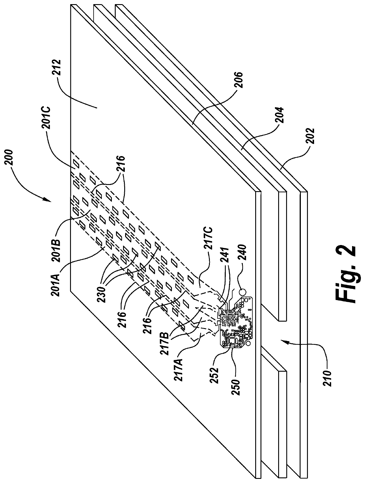
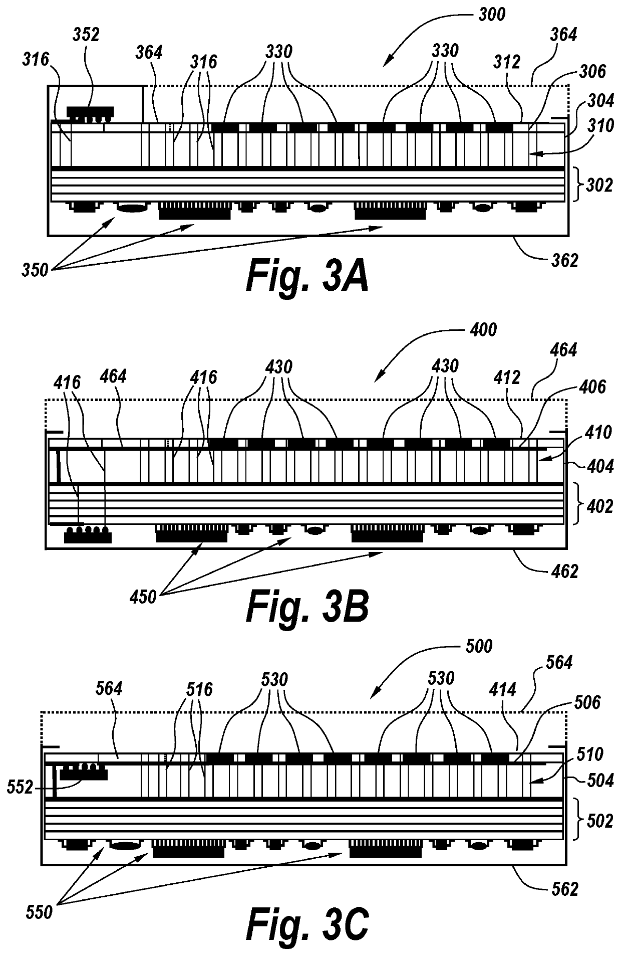
[0022]According to the present disclosure, automotive radar sensor modules are provided with a low-cost solution for the antenna(s) and RF front end based on low-cost commonly used laminates, such as FR4, to perform at higher frequencies used in automotive radar solutions, e.g., 24 GHz and / or 76-81 GHz, without the need to utilize high-cost, high-frequency substrates. This solution can also include the digital circuitry in a single-board format and, hence, provide a compact complete solution. According to the exemplary embodiments, since the more expensive laminate materials, such as Astra® MT77, Rogers RO3003 or RO4350, or other similar materials are not used, and only standard printed circuit board fabrication techniques are required, the cost and complexities of fabrication are significantly reduced, while the RF performance is maintained or improved.

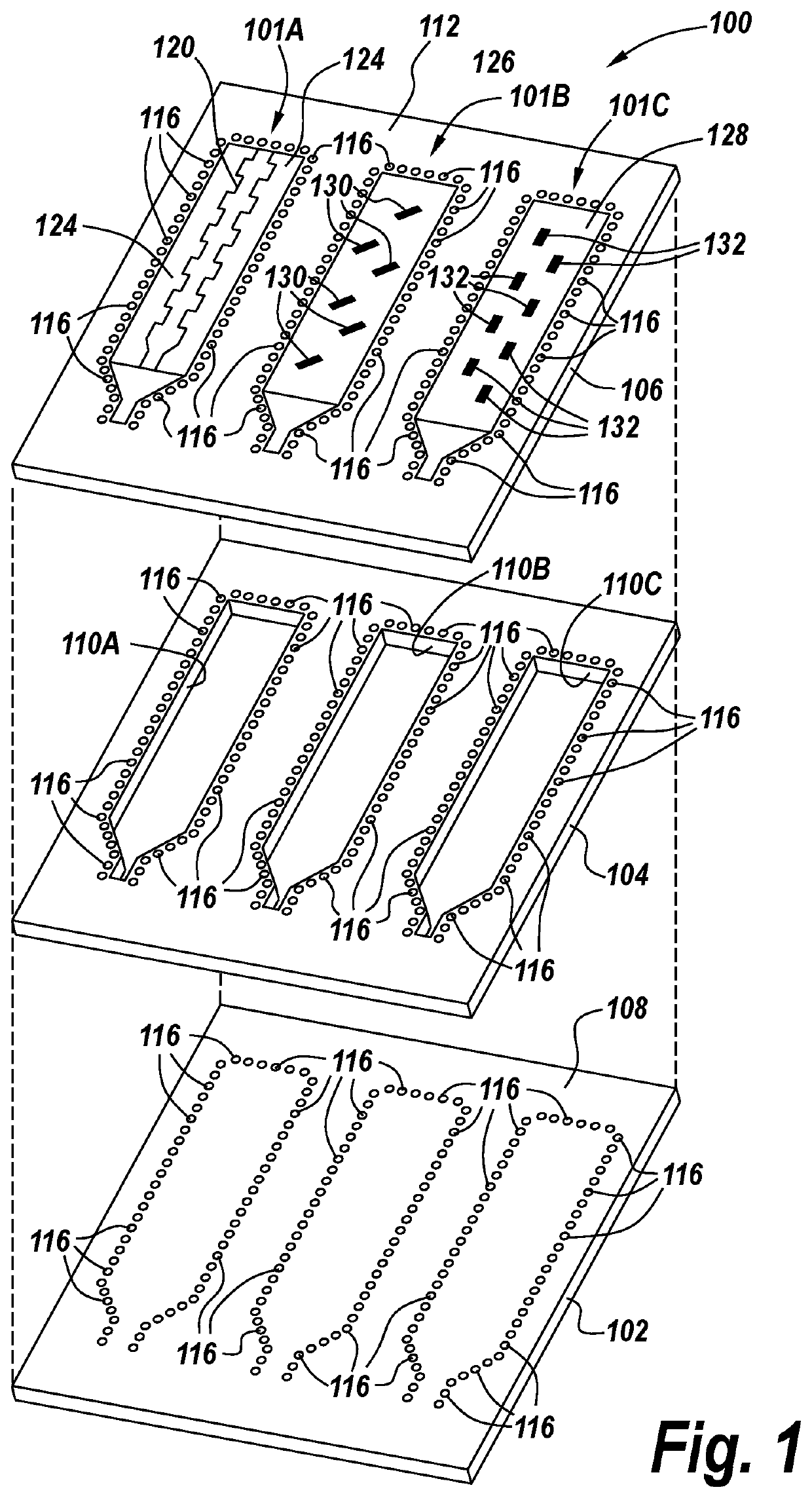
[0023]According to the present disclosure, waveguides such as rectangular waveguides are structured by stacking laminates or layers...


PUM

PropertyMeasurementUnit
frequenciesaaaaaaaaaa
thicknessaaaaaaaaaa

Abstract

A waveguide antenna apparatus includes a lower laminate layer of non-radio-frequency (RF) material and a first layer of conductive material formed on a top surface of the lower laminate layer of non-RF material. A middle layer of non-RF material formed over the first layer of conductive material, the middle layer of non-RF material comprising a waveguide cavity formed through the middle layer of non-RF material, such that air forms a propagation medium for radiation in the waveguide cavity. An upper layer of non-RF material is formed over the middle layer of non-RF material, and a second layer of conductive material is formed on a top surface of the upper layer of non-RF material, the first and second layers of conductive material and the waveguide cavity being part of a waveguide antenna.

Description

BACKGROUND1. Technical Field[0001]The present disclosure is related to radar detection systems and, in particular, to an antenna system for an automotive radar system using low-cost non-radio-frequency (RF) laminate materials for the antenna structure and / or RF front end, and an automotive radar system utilizing the same.2. Discussion of Related Art[0002]In conventional automotive radar sensor modules, electronic components are mounted on a printed circuit board (PCB). For example, both transmit (Tx) and receive (Rx) antenna components can be implemented by forming arrays of antenna “patches” on the surface of the PCB. These patches, as well as associated components such as feed lines, strip lines, waveguides and RF transition elements, e.g., waveguide-to-microstrip line transitions, are commonly formed by depositing metal and / or other conductive material on the surface of the PCB in a predetermined desired pattern.[0003]Typically, PCBs are made of any standard inexpensive PCB mater...

Claims


Application Information

Patent Timeline
Patent Type & Authority Patents(United States)
IPC IPC(8): H01Q13/06H01Q1/42H01Q13/18H01Q23/00
CPCH01Q13/06H01Q1/422H01Q13/18H01Q23/00H01P3/121H01P5/107H01Q9/0457H01Q21/0043
Inventor AHMADLOO, MAJID
Owner VEONEER US LLC
Why Eureka
Try Eureka