
Capacitor interposer layer (CIL) in a die-to-wafer three-dimensional (3D) integrated circuit (IC) (3DIC)

a three-dimensional, integrated circuit technology, applied in the direction of fixed capacitors, structural fixed capacitor combinations, inductances, etc., can solve the problems of high-performance ics being vulnerable to excessive voltage drop in the power distribution network, pressure to change the geometries of ics, etc., to reduce pdn voltage droop, reduce equivalent series resistance (esr) and equivalent series inductance (esl). , the effect of low profil

Active Publication Date: 2021-10-26
QUALCOMM INC
View PDF10 Cites 1 Cited by
  • Summary
  • Abstract
  • Description
  • Claims
  • Application Information

AI Technical Summary

Benefits of technology

The patent describes a way to create a layer of capacitors in a 3D integrated circuit. This layer is placed close to the area where power is distributed in the circuit, which helps to reduce resistance and inductance and allows for a more efficient and compact device. The method involves using a copper-to-copper bond to connect the wafer and the chip, which also reduces voltage droop in the power distribution network. Overall, this technique leads to improved performance and reduced size of the integrated circuit.

Problems solved by technology

As the size of many computing devices shrink, there has been pressure to change the geometries of the ICs.
However, such high-performance IC may be vulnerable to excessive voltage drop in a power distribution network extending between the battery of the computing device and the IC where voltage drop may be caused, at least in part, by equivalent series resistance (ESR) and / or equivalent series inductance (ESL) of the conductors between the battery and the internal power origin within the IC.

Method used


Image

  • Capacitor interposer layer (CIL) in a die-to-wafer three-dimensional (3D) integrated circuit (IC) (3DIC)
  • Capacitor interposer layer (CIL) in a die-to-wafer three-dimensional (3D) integrated circuit (IC) (3DIC)
  • Capacitor interposer layer (CIL) in a die-to-wafer three-dimensional (3D) integrated circuit (IC) (3DIC)

Examples


Embodiment Construction

[0019]With reference now to the drawing figures, several exemplary aspects of the present disclosure are described. The word “exemplary” is used herein to mean “serving as an example, instance, or illustration.” Any aspect described herein as “exemplary” is not necessarily to be construed as preferred or advantageous over other aspects.

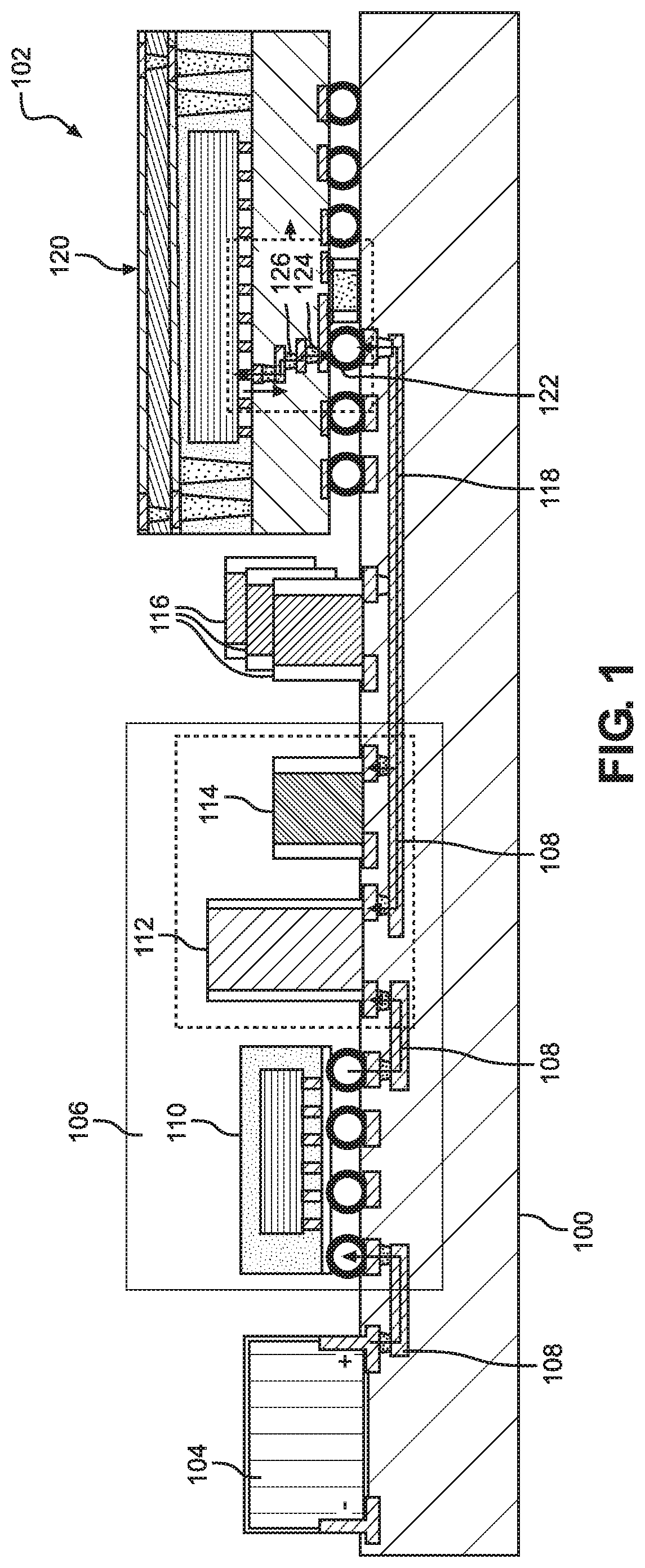
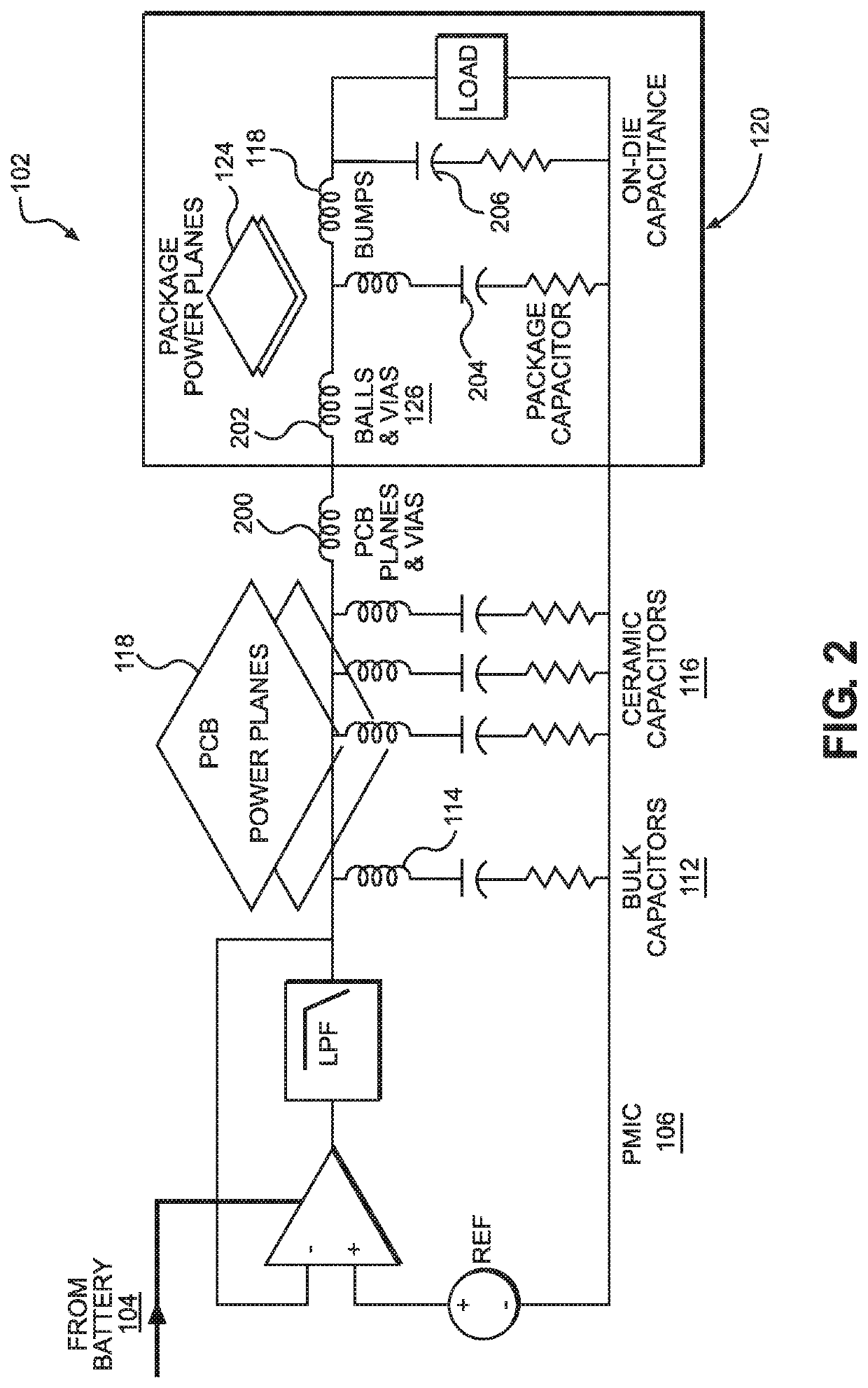
[0020]Aspects disclosed in the detailed description include a capacitor interposer layer (CIL) in a die-to-wafer three-dimensional (3D) integrated circuit (IC) (3DIC) and methods of forming the same. In an exemplary aspect, a CIL is formed in a wafer under a power distribution network (PDN) die area of a chip. Electrical connections between the wafer and the chip are formed using a copper-to-copper bond. This placement allows a capacitor to be close to the PDN die area within the chip to reduce equivalent series resistance (ESR) and equivalent series inductance (ESL), while permitting a relatively low profile device with reduced PDN voltage droop.

[002...


PUM


Abstract

A capacitor interposer layer (CIL) in a die-to-wafer three dimensional integrated circuit (3DIC) and methods of forming the same are disclosed. A CIL is formed in a wafer under a power distribution network (PDN) die area of a chip. Electrical connections between the wafer and the chip are formed using a copper-to-copper bond. This placement allows the capacitor to be close to the PDN die area within the chip to reduce equivalent series resistance (ESR) and equivalent series inductance (ESL), while permitting a relatively low profile device with reduced PDN voltage droop.

Description

BACKGROUNDI. Field of the Disclosure[0001]The technology of the disclosure relates generally to integrated circuits (IC) and, more particularly, to providing a capacitor in an interposer layer between a die and a wafer of an IC.II. Background[0002]Computing devices typically rely on integrated circuits (ICs) to handle various functions. As the size of many computing devices shrink, there has been pressure to change the geometries of the ICs. One such change in the geometry is a three-dimensional (3D) IC (3DIC), where a chip may be stacked on top of a wafer. Such arrangement may be desirable to conserve space. However, such high-performance IC may be vulnerable to excessive voltage drop in a power distribution network extending between the battery of the computing device and the IC where voltage drop may be caused, at least in part, by equivalent series resistance (ESR) and / or equivalent series inductance (ESL) of the conductors between the battery and the internal power origin withi...

Claims


Application Information

Patent Timeline
IPC IPC(8): H01L23/00H01L49/02H01L23/48H01L21/768H01L27/01H01L25/18H01L25/00H01L21/288H01L21/311H01L21/56
CPCH01L24/08H01L21/288H01L21/31111H01L21/565H01L21/76802H01L21/76877H01L23/481H01L24/05H01L24/13H01L24/89H01L25/18H01L25/50H01L27/01H01L28/90H01L2224/0557H01L2224/05647H01L2224/08147H01L2224/13025H01L2224/13147H01L2224/80895H01L2924/19011H01L2924/19041H01L23/3128H01L28/10H01L25/16H01L23/64H01L23/49816H01L23/49833H01L23/50H01L23/5383H01G4/40H01G4/385H01L2224/16225H01L2924/15184H01L2924/15192H01L2924/181H01L2924/19106H01L2924/19103H01L2924/19104H01L2924/14H01L2224/08225H01L24/80H01L2224/12105H01L2224/0401H01L2224/13022H01L2224/11334H01L2224/06181H01L2224/04105H01L24/92H01L24/94H01L2224/08265H01L2224/73201H01L2224/80896H01L2224/94H01L2224/9202H01L24/11H01L2224/80006H01L2224/80357H01L2224/08145H01L2224/08146H01L2924/00012H01L2924/00014H01L2224/80001H01L2224/11H01L2224/08H01L2224/13
Inventor LAN, JE-HSIUNGKIM, JONGHAEKIM, JINSEONGCHIDAMBARAM, PERIANNAN
Owner QUALCOMM INC
Learn More