
Near-infrared absorbing composition, optical structure, and camera module and electronic device comprising the same

a composition and near-infrared technology, applied in the direction of pictoral communication, electrical apparatus, group 5/15 element organic compounds, etc., to achieve excellent near-infrared absorption, minimize optical distortion, and low visible absorption

Active Publication Date: 2021-11-02
SAMSUNG ELECTRONICS CO LTD
View PDF12 Cites 0 Cited by
  • Summary
  • Abstract
  • Description
  • Claims
  • Application Information

AI Technical Summary

Benefits of technology

The near-infrared absorbing composition described in this patent has great properties for absorbing near-infrared light and minimizing the absorption of visible light. This results in a clear image with minimal distortion. Additionally, the composition has good solubility in organic solvents, making it easy to create a high-quality coating. This optical structure can be used in camera modules and electronic devices to provide images with minimal optical distortion.

Problems solved by technology

However, when the thin-film optical filter is used to observe and take a picture of a high luminance subject, it may cause a flare phenomenon such as a Wi-Fi-type flare phenomenon that an outline is generated around the subject, a petal flare phenomenon that light is irradiated with the subject as the center, and the like.

Method used


Image

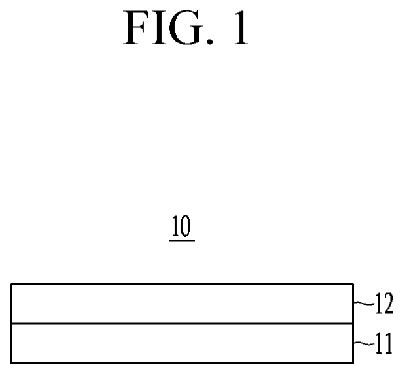
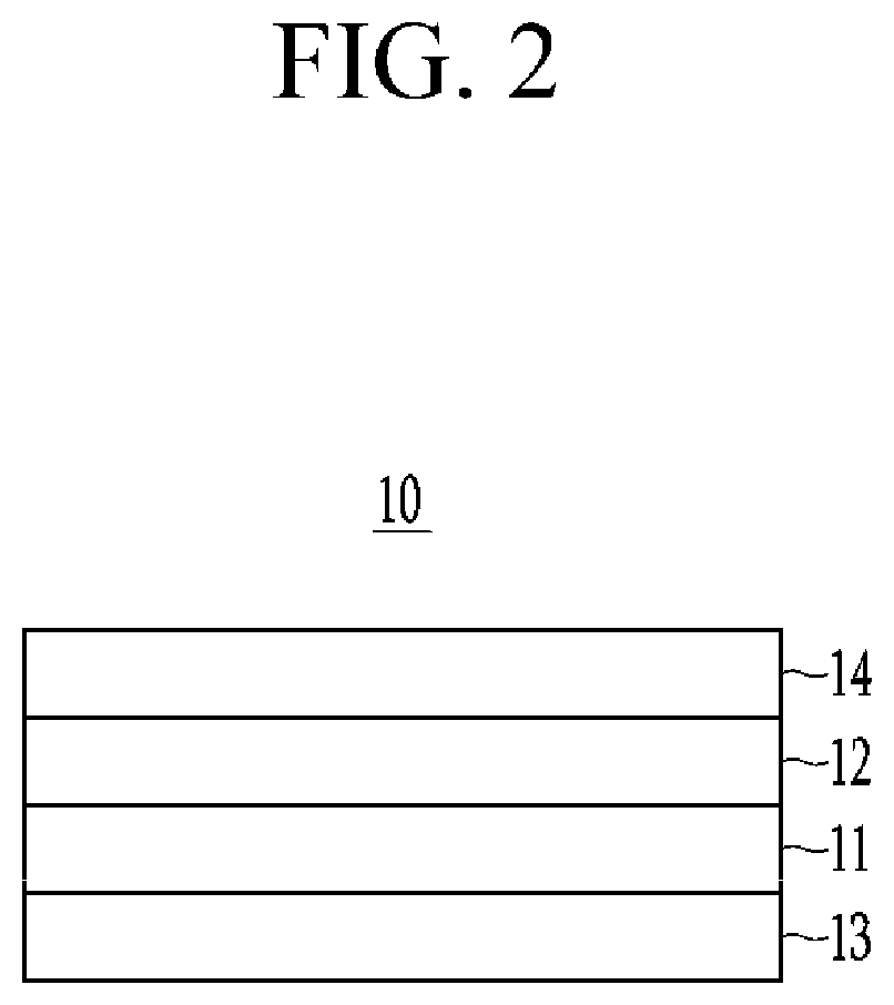
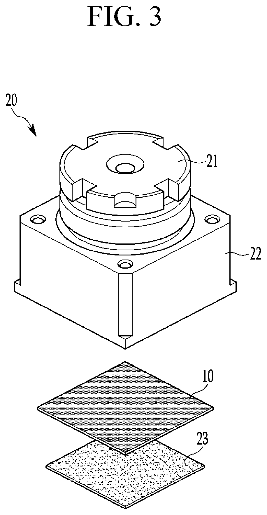
  • Near-infrared absorbing composition, optical structure, and camera module and electronic device comprising the same
  • Near-infrared absorbing composition, optical structure, and camera module and electronic device comprising the same
  • Near-infrared absorbing composition, optical structure, and camera module and electronic device comprising the same

Examples


preparation example 1

[0194]10 g of copper (II) acetate (Alfa Aesar) is dissolved in a tetrahydrofuran solvent using a magnetic stirrer, 6.28 g of trifluoromethylacetic acid is added thereto, and the mixture is reacted at room temperature for 1 day. 6.06 g of methyl phosphate (a mono / di mixture, TCI Inc.) is added to the reaction solution, and the mixture is reacted at room temperature for 1 day. A nonreactant particle in the reaction solution is removed through a syringe filter, about ½ of tetrahydrofuran is removed with a rotary evaporator, and a precipitate is obtained therefrom by using hexane, and filtered, and dried at room temperature to 50° C. in a vacuum oven for 12 hours to prepare a copper complex represented by Chemical Formula 1-1.

[0195]

preparation example 2

[0196]A copper complex represented by Chemical Formula 1-2 is prepared according to the same method as Preparation Example 1 except for using 10 g of copper acetate, 6.28 g of trifluoromethyl acetic acid (TCI Inc.), and 7.75 g of ethylphosphate (a mono / di mixture, TCI Inc.).

[0197]

preparation example 3

[0198]A copper complex represented by Chemical Formula 1-3 is prepared according to the same method as Preparation Example 1 except for using 10 g of copper acetate, 6.28 g of trifluoromethyl acetic acid (TCI Inc.), and 11.03 g of isopropyl phosphate (TCI Inc.).

[0199]


PUM

PropertyMeasurementUnit
absorption wavelengthaaaaaaaaaa
thicknessaaaaaaaaaa
thicknessaaaaaaaaaa

Abstract

Disclosed are a near-infrared absorbing composition, an optical structure, and a camera module and an electronic device including the same, wherein the near-infrared absorbing composition includes a copper complex represented by Chemical Formula 1:(L1)-Cu-(L2)n  [Chemical Formula 1]Wherein in Chemical Formula 1, L1, L2, and n are described in the detailed description.

Description

CROSS-REFERENCE TO RELATED APPLICATION[0001]This application claims priority to and the benefit of Korean Patent Application No. 10-2018-0060401, filed in the Korean Intellectual Property Office on May 28, 2018, the entire contents of which are incorporated herein by reference.BACKGROUND1. Field[0002]A near-infrared absorbing composition, an optical structure, and a camera module and an electronic device including the same are disclosed.2. Description of the Related Art[0003]Recently, an electronic device including an image sensor that stores an image as an electrical signal, such as a cell phone, a digital camera, a camcorder and a camera, has been widely used.[0004]This electronic device may include an optical filter having a near-infrared absorption capability in order to reduce or prevent generation of an optical distortion by light in the other regions than a visible region.[0005]The optical filter is generally mounted in front of an image sensor of a camera module and thus pla...

Claims


Application Information

Patent Timeline
Patent Type & Authority Patents(United States)
IPC IPC(8): C07F9/09H04N5/225C03C17/32C09D5/32C07F9/12C09D133/00C09D163/00C08K5/56
CPCC09D5/32C03C17/326C07F9/095C07F9/12C09D133/00C09D163/00H04N5/2254C03C2217/74C08K5/56C07F9/091C07F9/11C09D7/63C08K5/0091C03C17/009C08G59/688H04N23/55C09K3/00C07F1/08C08K5/02C08K5/521C08K5/41C08L101/06G02B5/22G02B5/281
Inventor KIM, MI JEONGKO, YOON SEOKWON, JONG HOONJUNG, MYUNGSUPBYUN, SUN JUNG
Owner SAMSUNG ELECTRONICS CO LTD
Learn More