Semiconductor device and production method

a semiconductor device and production method technology, applied in the direction of semiconductor devices, basic electric elements, electrical equipment, etc., can solve the problems of complex process, rounded corners, and precise reproduction, and achieve the effect of suppressing the current concentration at the corners of the trenches and easy formation

Active Publication Date: 2021-11-02
TOYODA GOSEI CO LTD
View PDF12 Cites 0 Cited by
  • Summary
  • Abstract
  • Description
  • Claims
  • Application Information

AI Technical Summary

Benefits of technology

[0009]In view of the foregoing, one object of the present invention is to provide a Group III nitride semiconductor device that suppresses current concentration at the corners of the trench. The other object of the present invention is to provide a method for producing a semiconductor device by which a recess having a small pattern can be formed on a Group III nitride semiconductor layer.
[0016]In the present invention, a diameter of an inscribed circle of the regular hexagon of the planar pattern of the recess is preferably 0.8 μm to 2.0 μm. Within this range, hydrogen can be efficiently removed from the recess during heat treatment for activating the p-type layer. Moreover, the unit cell size can be reduced, and the side wall area of the trench can be enlarged, thereby improving the electrical characteristics.
[0017]In the present invention, the side wall of the trench is preferably an a-plane, and the side wall of the recess is preferably a m-plane. Thereby, the reproducibility of the planar patterns of the trench and the recess is improved.
[0025]The depth of the groove is preferably 0.2 μm to 0.5 μm to improve the reproducibility of the groove pattern and more easily form the groove.
[0026]The sides of the regular hexagon of the photomask are preferably parallel to the m-axis direction or a-axis direction of the semiconductor layer to improve the reproducibility of the groove pattern and more easily form the groove.
[0028]According to the present invention, current concentration at the corners of the trench can be suppressed. According to the method for producing a semiconductor device of the other invention, a groove having a small pattern can be easily formed on the Group III nitride semiconductor layer.

Problems solved by technology

However, the recess pattern is small, and thus cannot be precisely reproduced due to the limit of the photolithography resolution, resulting in rounded corners.
However, the formation of the structure disclosed in Patent Document 1, requires regrowth of semiconductor layer or ion implantation, and thus the process was complicated.
There was also a problem that when plane distribution of the hole concentration was constant in the low-concentration p-type region surrounding the side wall of the trench, current was concentrated at the corners of the trench.

Method used


Image

  • Semiconductor device and production method
  • Semiconductor device and production method
  • Semiconductor device and production method

Examples


first embodiment

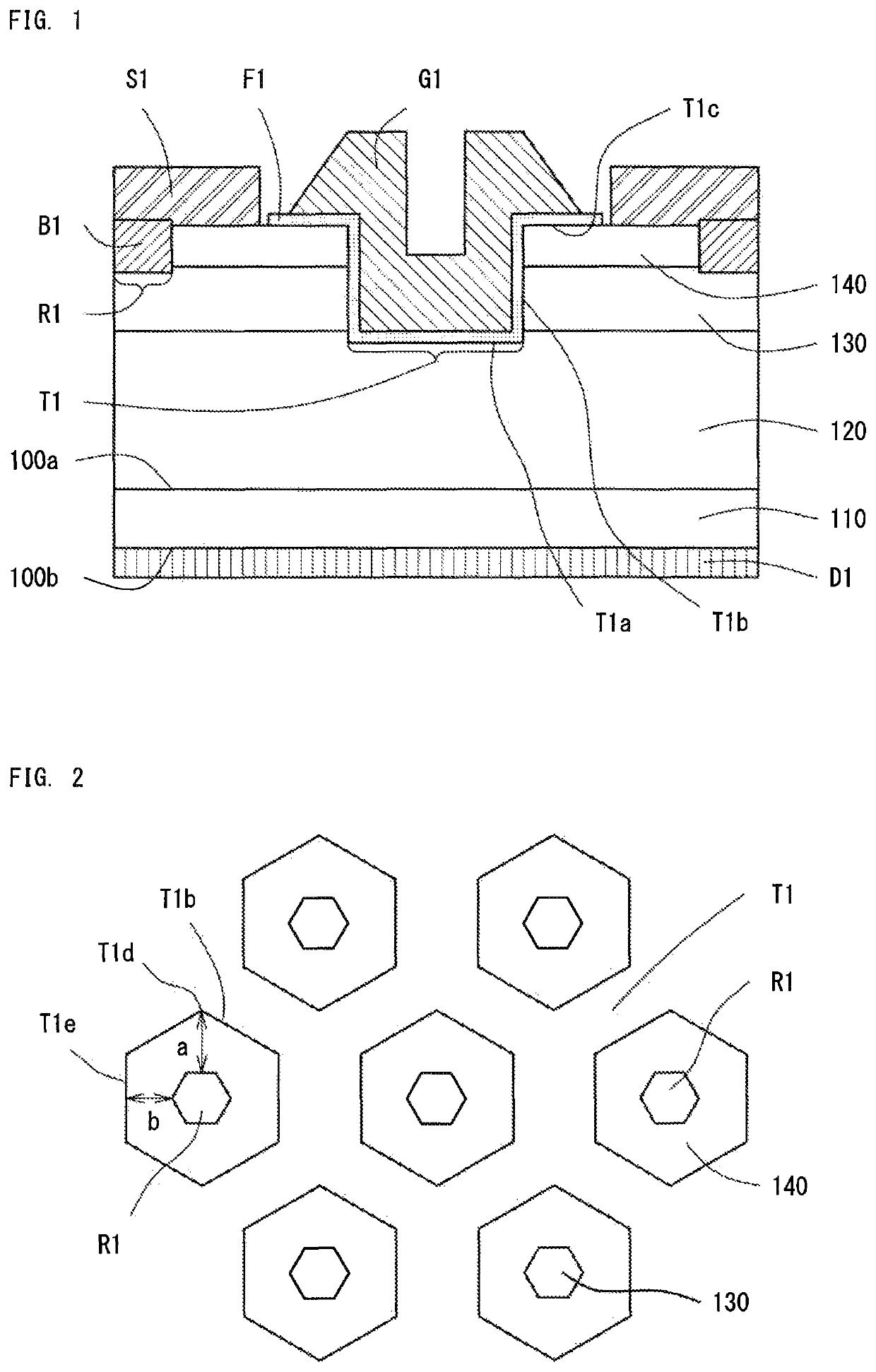
[0041]FIG. 1 is a view showing the structure of a semiconductor device according to a first embodiment. As shown in FIG. 1, the semiconductor device according to the first embodiment is a trench gate type FET, which includes a substrate 110, a first n-type layer 120, a p-type layer 130, a second n-type layer 140, a trench T1, a recess R1, a gate insulating film F1, a gate electrode G1, a source electrode S1, a body electrode B1, and a drain electrode Dl.

[0042]The substrate 110 is a flat substrate made of Si-doped n-GaN having a c-plane main surface and having a thickness of 300 μm. The Si concentration is 1×10¹⁸ / cm3. The substrate may be made of any conductive material capable of being used as a growth substrate for a Group III nitride semiconductor. For example, ZnO and Si may be used. However, in terms of lattice matching, a GaN substrate is preferably used as in the present embodiment.

[0043]The first n-type layer 120 is a Si-doped n-GaN layer having a c-plane main surface, deposi...

second embodiment

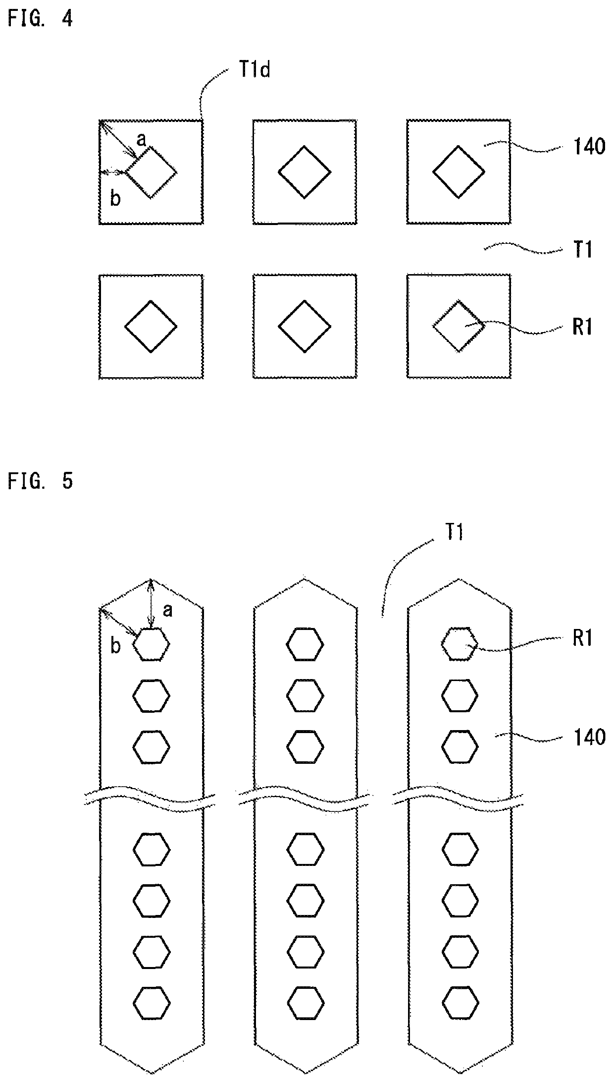
[0078]A second embodiment relates to a method for producing a recess R1 of the trench gate type vertical field effect transistor (FET) according to the first embodiment. The semiconductor device (FET) has the same structure as that shown in FIG. 1 of the first embodiment. The first n-type layer 120, the p-type layer 130, and the second n-type layer 140 in FIG. 1 correspond to the semiconductor layer in the invention of the production method.

[0079]In the production method in the second embodiment, a diameter of an inscribed circle of the regular hexagon of the recess R1 is preferably 0.8 μm to 2.0 μm. Such a small sized recess R1 has been difficult to form, but can be more easily formed by the production method according to the second embodiment. The diameter of the inscribed circle of the regular hexagon of the recess R1 is more preferably 0.9 μm to 1.5 μm, and further preferably 1.0 μm to 1.2 μm.

[0080]The recess R1 may have any depth as long as the depth reaches the p-type layer 13...


PUM

PropertyMeasurementUnit
diameteraaaaaaaaaa
depthaaaaaaaaaa
thicknessaaaaaaaaaa

Abstract

The present invention provides a Group III nitride semiconductor device in which current concentration at the corners of the trench is suppressed. The semiconductor device has a pattern in which regular hexagonal unit cells are arranged in a honeycomb pattern. The semiconductor layer is sectionalized into regular hexagonal patterns by the trench. The recess has a small regular hexagonal pattern contained in the regular hexagonal pattern of the semiconductor layer sectionalized by the trench, which is obtained by reducing the regular hexagon of the semiconductor layer with the same center. Moreover, the regular hexagonal pattern of the recess is rotated by 30° with respect to the regular hexagon of the semiconductor layer. The Mg activation ratio is lower in the vicinity of corners of the trench than that in other regions in the vicinity of side walls of the trench of the p-type layer.

Description

BACKGROUND OF THE INVENTIONField of the Invention[0001]The present invention relates to a Group III nitride semiconductor device, and a production method therefor.Background Art[0002]Patent Document 1 discloses that in a Group III nitride semiconductor trench gate type FET, a p-type region with a Mg concentration lower than that of the p-type layer is formed between the p-type layer and the side wall of the trench. Such a structure allows reducing the on voltage, thereby reducing the channel resistance.[0003]Patent Document 2 discloses a trench gate type FET having a planar pattern in which the unit cell is a regular hexagon and the unit cells are arranged in a honeycomb pattern. It also discloses a recess structure in which a groove (recess) for exposing the p-type layer is formed by removing a part of the n-type layer formed on the p-type layer, and an electrode is formed in contact with the p-type layer. The recess has a regular hexagonal pattern obtained by reducing the regular ...

Claims


Application Information

Patent Timeline
Patent Type & Authority Patents(United States)
IPC IPC(8): H01L29/423H01L29/66H01L29/808H01L29/20H01L29/78H01L27/105
CPCH01L29/4236H01L27/105H01L29/2003H01L29/66666H01L29/7827H01L29/8083H01L29/66522H01L29/401H01L29/42356H01L29/7813H01L29/0696H01L29/41766H01L29/66734H01L29/66727H01L29/045H01L29/7397
Inventor NISHII, JUNYA
Owner TOYODA GOSEI CO LTD
Why Eureka
Try Eureka