
III-nitride tunnel junction light emitting diode with wall plug efficiency of over seventy percent
a technology of iiinitride and tunnel junction, which is applied in the direction of solid-state devices, lasers, semiconductor lasers, etc., can solve the problems of low hole concentration and mobility, difficult electrical contact of p-gan, and inability to use p-gan as a current spreading layer, etc., to achieve less loss, improve efficiency, and reduce droop
- Summary
- Abstract
- Description
- Claims
- Application Information
AI Technical Summary
Benefits of technology
Problems solved by technology
Method used
Image

Examples
example 1
Transparent LED or PSS Lateral TJ LED Structure and Fabrication
[0061]A lateral LED is term used for LEDs that use ITO or ZnO for current spreading on the top layer.
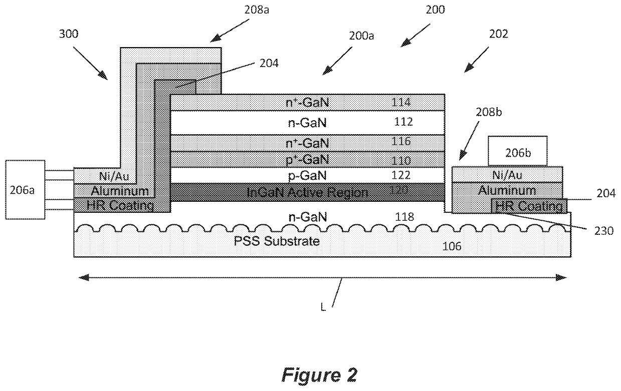
[0062]FIG. 2 illustrates the lateral tunnel junction LED 200 on a PSS substrate 106 and having a high reflective (HR) coating 204 under the wire bond pads 206a, 206b.
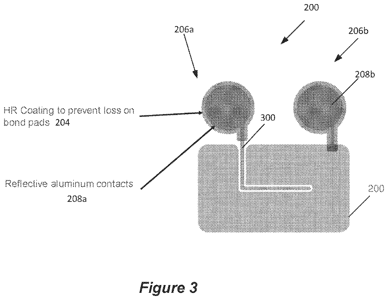
[0063]For the transparent LEDs 200 according to an embodiment of the present invention, a mesa 202 etch was first done using reactive ion etching (RIE) with SiCl4. A dielectric coating 204 was then deposited to reduce optical loss of the wire bond pads 206a, 206b. In one embodiments, the dielectric coating 204 comprises seven-layer dielectric stack consisting of Al2O3 / Ta2O5 / SiO2 was designed using TFCalc which increased the reflectivity of the wire bond pads 206a, 206b to over 98% at a wavelength of 450 nm. The topside wire bond pad 206a was also moved off the mesa 202 to prevent it from reflecting light (emitted under it) back into the chip 200a. A 600 / 200 / ...
example 2
Transparent Substrate Embodiment
[0069]FIG. 6 illustrates an embodiment wherein a transparent substrate is used to hold the LED. In an alternative embodiment, multiple LEDs could be used on the same substrate,
example 3
Back Reflector Embodiment
[0070]FIG. 7 illustrates a device embodiment 700 wherein a back reflector 702 (e.g., metal such as silver or aluminum) is used on the sapphire 106 to prevent loss on the header 406, and high reflective dielectric coating 704 is between the back reflector 702 (e.g., aluminum) and the substrate 106. Wire bonds 710 are also shown.
[0071]FIG. 8(a) shows the measured LIV characteristic (plotting light output power and voltage as a function of current) for the lateral TJ LED embodiment with back reflector illustrated in FIG. 7, wherein current is injected into an area of 0.1 mm2 (so that 1 mA drive current corresponds to 1 A / cm2 current density), FIG. 8(b) plots the measured EQE and WPE for this lateral tunnel junction LED embodiment (peak EQE is 78% and peak WPE is 72%).
PUM
| Property | Measurement | Unit |
|---|---|---|
| EQE | aaaaa | aaaaa |
| drive current density | aaaaa | aaaaa |
| EQE | aaaaa | aaaaa |
Abstract
Description
Claims
Application Information