
Method for manufacturing circuit board

a technology of circuit board and manufacturing method, which is applied in the direction of printed circuit, printed circuit, printed circuit simultaneous processing, etc., can solve the problems of reduced circuit board size, increased manufacturing cost, and difficulty in transportation, so as to reduce manufacturing costs and improve product yield, the effect of saving costs

Active Publication Date: 2021-11-16
HO CHUNG W
View PDF6 Cites 0 Cited by
  • Summary
  • Abstract
  • Description
  • Claims
  • Application Information

AI Technical Summary

Benefits of technology

The invention provides a method for manufacturing a circuit board that is safer, simpler, and more cost-effective. The method involves applying a stainless steel layer on a first conductive layer of a first carrier board using sputtering, which separates the manufactured product board from the carrier board. This stainless steel layer is lightweight and easy to operate with, and the first carrier board can be reused, thereby reducing manufacturing costs. These technical effects make the method safer, simpler, and more efficient for manufacturing circuit boards.

Problems solved by technology

However, in the well-known coreless manufacturing process, since some of the carrier board and some of the circuit board require to be cut off, the size of the circuit board may be reduced and the cut-off carrier board cannot be reused, resulting in increased manufacturing costs.
However, since the stainless steel board is of a large volume and a heavy weight, during the manufacturing process, transportation may often be difficult.
Moreover, edges and corners thereof are relatively sharp, often causing damage to the substrate per se or the machine.

Method used


Image

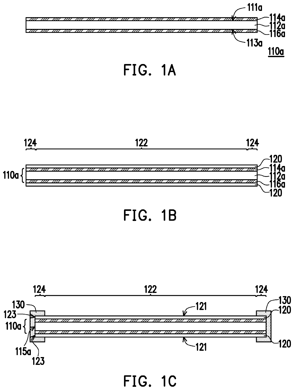
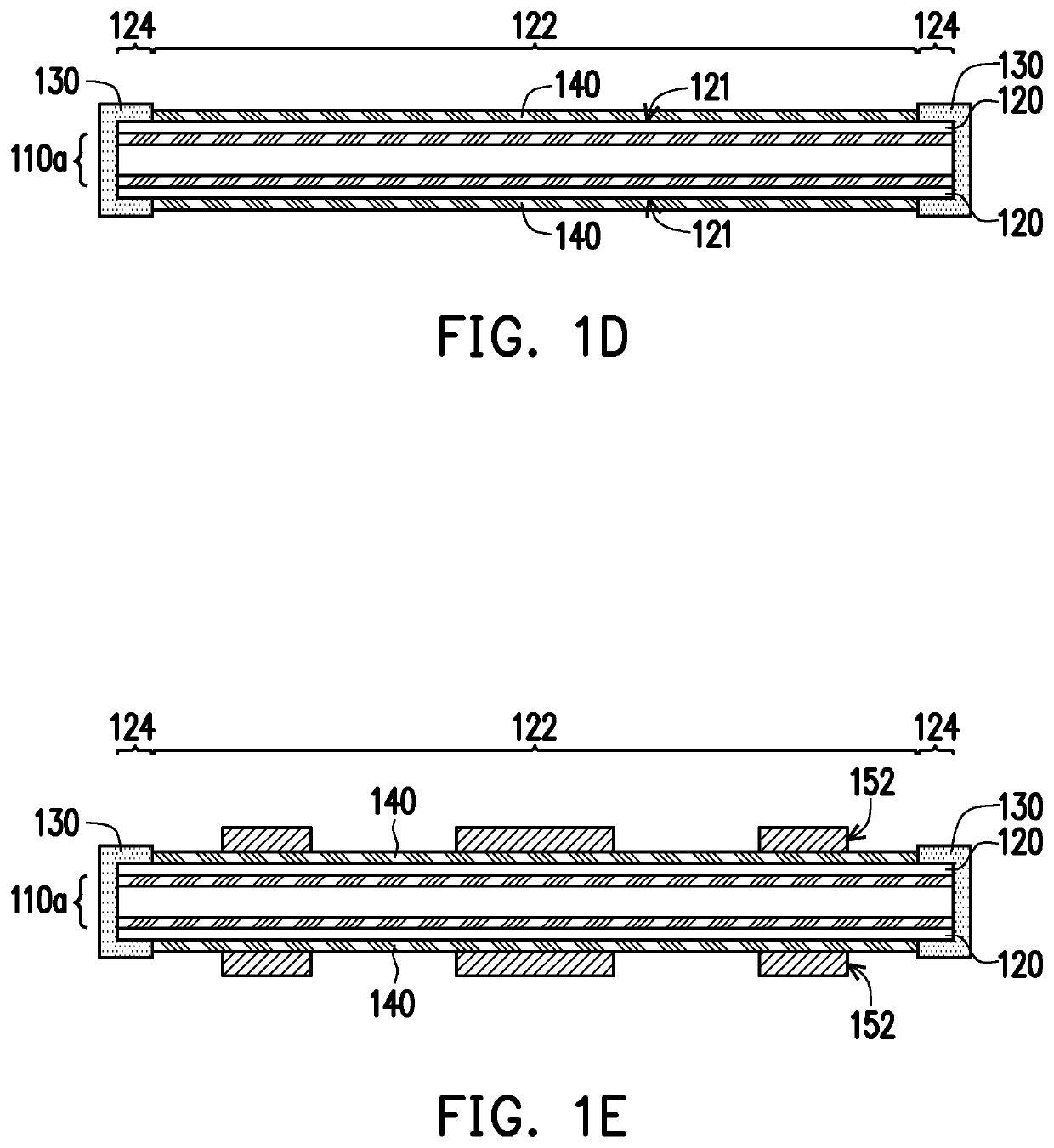
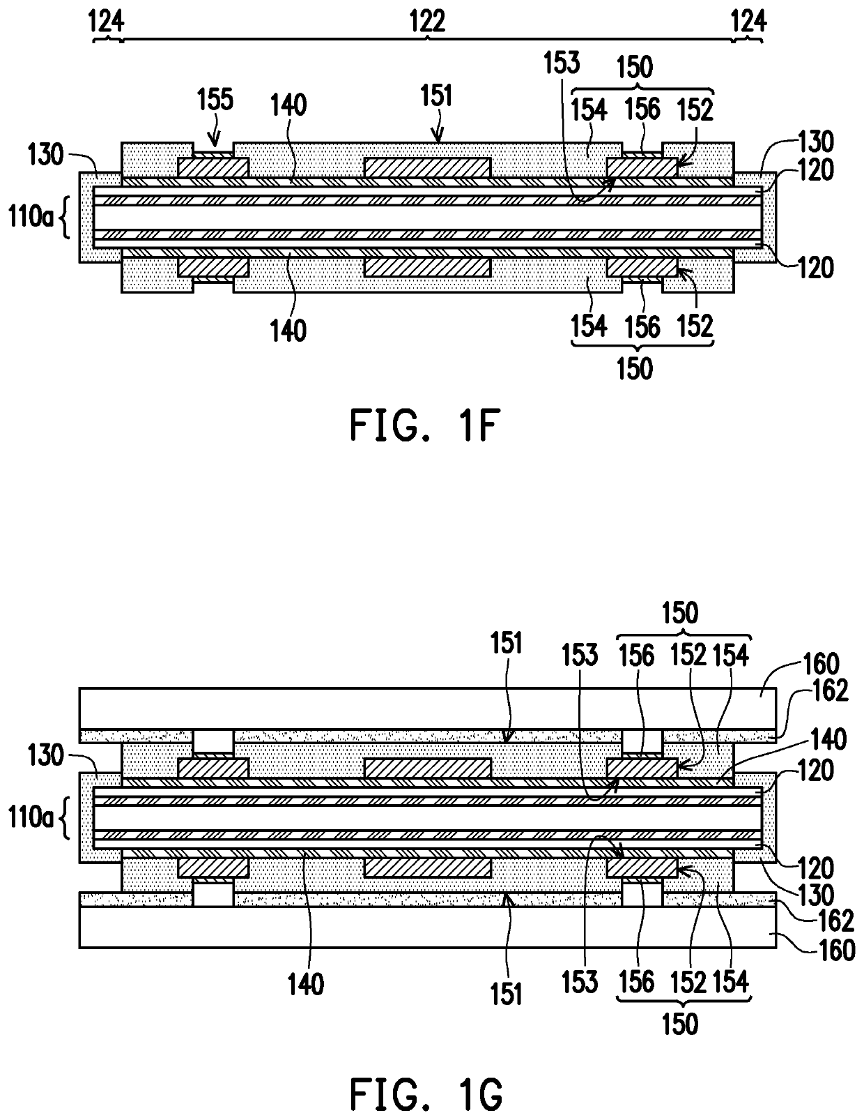
  • Method for manufacturing circuit board
  • Method for manufacturing circuit board
  • Method for manufacturing circuit board

Examples


Embodiment Construction

[0023]Reference will now be made in detail to the exemplary embodiments of the invention, examples of which are illustrated in the accompanying drawings. Wherever possible, the same element symbols are used in the drawings and description to represent the same or similar parts.

[0024]FIG. 1A to FIG. 1I are schematic cross-sectional views of a method for manufacturing a circuit board of an embodiment of the invention. Regarding the manufacturing method of the circuit board of this embodiment, first, referring to FIG. 1A, a first carrier board 110a having a substrate 112a and a first conductive layer 114a is provided. The substrate 112a has a first surface 111a, and the first conductive layer 114a is located on the first surface 111a. In this embodiment, the first carrier board 110a further includes a second conductive layer 116a. The substrate 112a has a second surface 113a opposite to the first surface 111a, and the second conductive layer 116a is located on the second surface 113a. ...


PUM

PropertyMeasurementUnit
thicknessaaaaaaaaaa
thicknessaaaaaaaaaa
thicknessaaaaaaaaaa

Abstract

A manufacturing method of a circuit board is provided. A first carrier board included a substrate and a first conductive layer is provided, and the first conductive layer is located on a first surface of the substrate. A stainless steel layer is sputtered on the first conductive layer. An insulating layer is formed to cover a peripheral region of the stainless steel layer and expose a central region. A circuit structure layer is formed on the central region exposed by the insulating layer. A bottom surface of the circuit structure layer is connected to the first carrier board. A transferring procedure is performed to adhere a top surface of the circuit structure layer onto an adhesive layer of a second carrier board. The first carrier board is separated with the circuit structure layer to transfer the circuit structure layer onto the second carrier board, and expose the bottom surface of the circuit structure layer. The manufacturing method of the circuit board of the present invention is safer and simpler, may effectively reduce the manufacturing costs and improve the product yields.

Description

TECHNICAL FIELD[0001]The invention relates to a method for manufacturing a board, and particularly to a method for manufacturing a circuit board.DESCRIPTION OF RELATED ART[0002]In the well-known coreless manufacturing process, part of the edge of the carrier board and part of the edge of the circuit board are first bonded with adhesive or copper-plated edge sealing. In another convention, a thin substrate (with a thickness of 100 μm, for example) containing a glass fiber cloth and, on each of both sides, being adhered with a piece of copper foil and a peelable ultra-thin copper foil (with a thickness of 3 μm to 5 μm, for example) attached thereon is employed as a carrier board. After the circuit board undergoes several processes, the part with adhesive or copper-plated edge sealing between the carrier board and the circuit board is cut off to obtain the circuit board for packaging process. However, in the well-known coreless manufacturing process, since some of the carrier board and...

Claims


Application Information

Patent Timeline
Patent Type & Authority Patents(United States)
IPC IPC(8): H05K3/10H05K3/00
CPCH05K3/10H05K3/00H05K3/205H05K3/0097H05K2203/0156H05K3/007H05K3/0011
Inventor HO, CHUNG W.
Owner HO CHUNG W
Learn More