Semiconductor device and method for driving the same

a technology of semiconductor devices and semiconductors, applied in the direction of pulse techniques, electronic switching, emergency protective circuit arrangements, etc., can solve the problems of increasing the chip size and substrate area of the mosfet, complicated assembly, and increasing the complexity of the substrate wiring pattern, so as to reduce the size and cost of the semiconductor device

Active Publication Date: 2022-01-04
MITSUBISHI ELECTRIC CORP
View PDF17 Cites 1 Cited by
  • Summary
  • Abstract
  • Description
  • Claims
  • Application Information

AI Technical Summary

Benefits of technology

[0006]To solve the problem, it is an object of the present invention to provide a technique for reducing the size and cost of a semiconductor device.
[0008]Such a configuration reduces the size and cost of the semiconductor device.

Problems solved by technology

In the discrete form, a large number of components cause more complicated assembly and a more complicated pattern of substrate wiring.
Unfortunately, variations in element property can cause timing shifts between the turn-on and turn-off operations of the IGBT and the MOSFET in a practical product.
Unfortunately, this increases the chip size and substrate area of the MOSFET, and by extension, increases cost.
Such a problem is found not only in the IGBT and the MOSFET, but also in the power semiconductor switching elements with operational properties different from each other.

Method used


Image

  • Semiconductor device and method for driving the same
  • Semiconductor device and method for driving the same
  • Semiconductor device and method for driving the same

Examples


first preferred embodiment

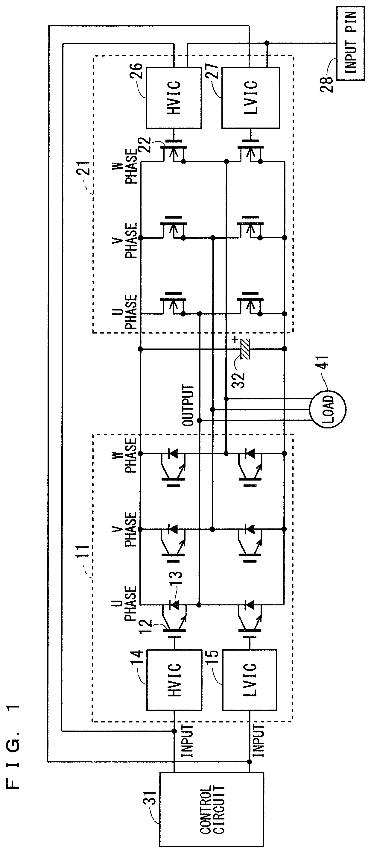
[0017]FIG. 1 is a circuit diagram illustrating the configuration of a semiconductor device according to a first preferred embodiment of the present invention. The semiconductor device in FIG. 1 includes a first power semiconductor module, which in this preferred embodiment is an insulated-gate bipolar transistor (IGBT) module 11, a second power semiconductor module, which in this preferred embodiment is a metal-oxide-semiconductor field-effect transistor (MOSFET) module 21, a control circuit 31, and an electrolytic capacitor 32.

[0018]The control circuit 31 is a microcomputer for instance, and controls the IGBT module 11 and the MOSFET module 21.

[0019]The IGBT module 11 and the MOSFET module 21 have inputs connected to the control circuit 31. The IGBT module 11 and the MOSFET module 21 have outputs connected to a load 41, such as a motor. In this way, the MOSFET module 21 according to the first preferred embodiment is connected to the IGBT module 11 in parallel between the input and ...

second preferred embodiment

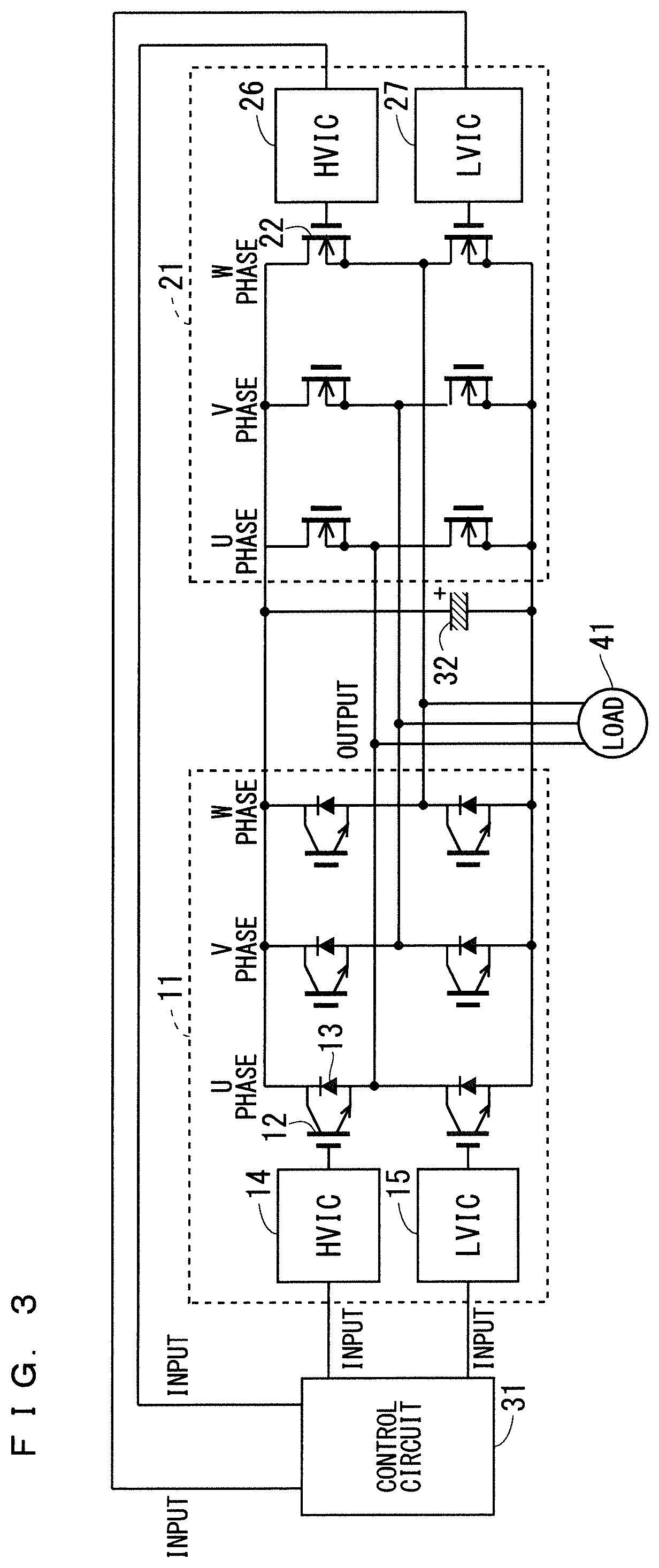
[0031]FIG. 3 is a circuit diagram illustrating the configuration of a semiconductor device according to a second preferred embodiment of the present invention. The same or similar components between the first and second preferred embodiments are denoted by the same reference signs. Thus, mainly described are components different between the preferred embodiments.

[0032]The MOSFET module 21 according to the second preferred embodiment does not include the input pin 28. Instead, the MOSFET module 21 according to the second preferred embodiment is connected to the IGBT module 11 in parallel between the control circuit 31 and the outputs of the IGBT module 11.

[0033]This enables the control circuit 31 to input, to the MOSFET module 21, a signal different from a signal input to the IGBT module 11. In the second preferred embodiment, the IGBT module 11 and the MOSFET module 21 can selectively execute the operation mode in response to the signal from the control circuit 31, which is describe...

third preferred embodiment

[0035]FIG. 4 is a side view of the configuration of a semiconductor device according to a third preferred embodiment of the present invention. The same or similar components between the third preferred embodiment and the first and second preferred embodiments are denoted by the same reference signs. Thus, mainly described are components different between the preferred embodiments.

[0036]The semiconductor device according to the third preferred embodiment includes a substrate 46 and a heat-dissipation fin 47 in addition to the components in the first or second preferred embodiment.

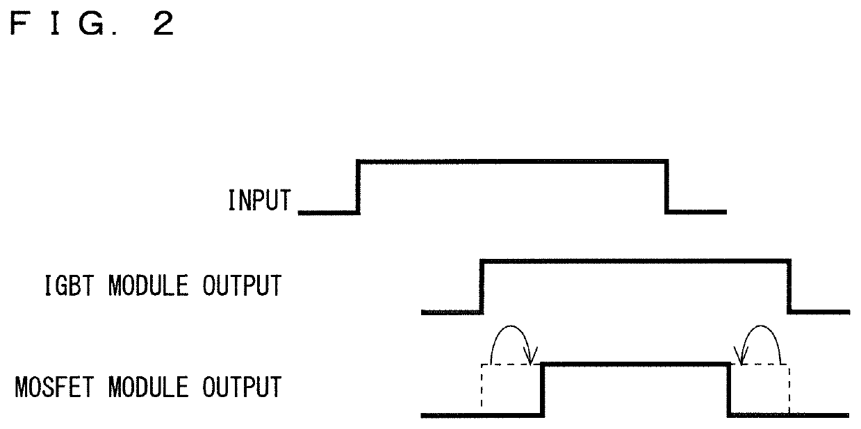
[0037]The IGBT module 11 and the MOSFET module 21 are disposed on one surface of the substrate 46. Here, the MOSFET module 21 has a switching loss of substantial zero in the configurations in the first and second preferred embodiments. In this case, the MOSFET module 21 has a relatively small package size or a relatively small rated current, have relatively little generated loss, and involves a relatively sm...


PUM

PropertyMeasurementUnit
timeaaaaaaaaaa
currentaaaaaaaaaa
sizeaaaaaaaaaa

Abstract

Provided is a technique for reducing the size and cost of a semiconductor device. A semiconductor device includes an IGBT module having an IGBT, and a MOSFET module having a MOSFET whose operational property is different from that of the IGBT, the MOSFET module being connected to the IGBT module in parallel. The semiconductor device is capable of selectively executing an operation mode in which switching timing in the IGBT module and switching timing in the MOSFET module are non-identical.

Description

BACKGROUND OF THE INVENTIONField of the Invention[0001]The present invention relates to semiconductor devices including power semiconductor switching elements and to methods for driving the same.Description of the Background Art[0002]Parallel connection between an insulated-gate bipolar transistor (IGBT) and a metal-oxide-semiconductor field-effect transistor (MOSFET) has been proposed as a technique for reducing loss generated in a power semiconductor element (e.g., Japanese Patent Application Laid-Open No. 2011-120330).[0003]Some semiconductor devices are constructed in a discrete form of power semiconductor elements; others are constructed in a semiconductor module form, such as packaged modules. In the discrete form, a large number of components cause more complicated assembly and a more complicated pattern of substrate wiring. On the other hand, in the semiconductor module form, design is performed to establish an independent output in a gate driver, to reflect restrictions on ...

Claims


Application Information

Patent Timeline
Patent Type & Authority Patents(United States)
IPC IPC(8): H02M7/493H02M1/088H02M1/32H02M7/00H01L23/367H01L25/18H01L27/02H02H1/00H02H3/02H02H3/16H03K17/082H03K17/28
CPCH02M7/493H02M1/088H01L23/367H01L25/18H01L27/0259H01L27/0266H02H1/0007H02H3/021H02H3/16H02M1/32H02M7/003H03K17/0828H03K17/28H03K17/12H01L25/074Y02B70/10H02M1/0051H02M1/0054H02M1/0095
Inventor SAKAI, SHINJI
Owner MITSUBISHI ELECTRIC CORP
Why Eureka
Try Eureka