Device and method for electron transfer from a sample to an energy analyzer and electron spectrometer device

a technology of electron spectrometer and energy analyzer, which is applied in the field of electron imaging apparatus and electron transfer method, can solve the problems of electron beam entering the energy analyzer with a marked divergence, imaging errors in the energy analyzer, and within relatively limited angle ranges, so as to enhance the efficiency of the energy analyzer, reduce aberration in the electron-optical system, and increase the electron angular range

Active Publication Date: 2022-05-10
SPECS SURFACE NANO ANALYSIS
View PDF21 Cites 0 Cited by
  • Summary
  • Abstract
  • Description
  • Claims
  • Application Information

AI Technical Summary

Benefits of technology

[0040]An important advantage of the invention therefore lies in the possibility of capturing substantially larger angular ranges of the electrons emitted from the sample. Since the relationship between the transverse momentum k1 and image angle α scales with the root of the energy:
[0041]k1˜sin α✓Ekin, at lower kinetic energies (e.g. equal to or less than 5 electron volts, such as in laser excitation, for example), angular intervals of more than + / −30° are possible and this considerably enhances the efficiency of the energy analyzer. Particular advantages of the invention also result from scanning of the second momentum coordinate to measure a two-dimensional momentum distribution and from the use of an imaging spin-filter. By positioning the deflector device in the first Gaussian image and focus of the second lens group, it is possible to achieve a parallel displacement of the momentum distribution image in the entry plane of the energy analyzer apparatus preferably with a single deflector unit, wherein the parallelism of the beam is preserved.
[0042]The aberrations of the combination of lens groups and deflector device can be advantageously reduced to the theoretically possible minimum, in that the image reciprocal to the desired momentum distribution image (i.e. the first Gaussian image of the source spot on the sample) is so small that the coding of the momentum distribution image is defined with extreme precision as a trajectory in this small Gaussian image. This characteristic distinguishes the present invention from all conventional beam transfer systems, in particular those according to [1, 2, 3, 4 and 5].
[0043]The inventors have found that, using the technique according to the invention, a concept realized in electron microscopy, in particular the creation of predetermined, very well focused real space images and reciprocal images in predetermined imaging planes using the optical image transition theorem, not only serves to reduce aberrations in the electron-optical system in electron spectroscopy but offers an additional substantial advantage: since the first Gaussian image can be displaced along the electron-optical axis by means of the first lens group, the tilt angle of the individual partial beams of the momentum distribution image can be minimized in the entry plane of the energy analyzer apparatus, without losing the beam position. This allows the deflection technique to be used for scanning the second momentum direction, in particular perpendicular to the entrance slit, even for high retardation conditions (ratio of the initial kinetic energy of the electrons on exit from the sample to the kinetic energy on entry into the energy analyzer apparatus). The preferred embodiment of the second lens group in the form of a zoom lens (lens that is configured for adjustment of an image magnification and preferably comprises five or more lens elements) makes it possible, in particular, to vary the image size and electron energy of the momentum image at the outlet from the electron imaging apparatus within broad limits and so adapt the momentum image size and energy to the desired conditions for the energy analyzer (energy resolution, momentum resolution).
[0044]The creation of the parallel image in the entry plane of the energy analyzer apparatus also advantageously simplifies a spin-resolved electron spectroscopy, since image errors on a spin-filter crystal at the outlet of the energy analyzer are reduced or avoided altogether.
[0045]A further particularly important advantage of the invention is that deflection of the momentum distribution image is simplified. Thus, in a preferred embodiment of the invention, it is provided that the deflector device only acts in a single plane perpendicular to the electron-optical axis. On transfer of the electrons along the electron-optical axis, the deflector device acts one single time, when the electrons pass through the space between the first lens group and the second lens group. This advantageously avoids conventional, complex double deflectors, e.g. according to [2], without having to accept imaging errors. Particularly preferably, the deflection plane of the deflector device and the first Gaussian plane (or another Gaussian plane, see below) coincide, so that an exact parallel displacement of the momentum distribution image in the second reciprocal plane is facilitated by actuating the deflector device. This completely avoids any additional beam tilting, such as is described in [3] and [5] for example.

Problems solved by technology

Although high angle resolutions were achieved in the past, this was only within relatively limited angle ranges.
Conventional transfer optics for angular-resolved measurement of electrons have a major disadvantage in that, at the outlet from the transfer optics and / or in the entry plane of the energy analyzer, the electron beam enters the energy analyzer with a marked divergence relative to the electron-optical axis, e.g. z-axis, of typically >10°.
It causes imaging errors in the energy analyzer and requires a significant amount of postprocessing effort to calculate energy- and angular distributions of the electrons.
Furthermore, conventional transfer optics do not have a sufficiently well focused and localized position space image of the sample source spot, from which the electrons are emitted (see e.g. [1]).
The divergence is particularly disadvantageous in the acquisition of the angular distribution along the second angular coordinate, wherein the second angular coordinate is sequentially scanned with the aid of one or two deflectors 20A′, 20B′ in the transfer optics (see [1], [2], [3], [4] and [5]).
With the scanning motion of the divergent beam perpendicular to the extent of the entrance slit, combination errors are created from the beam divergence in the entry plane in combination with aberrations induced by the deflection of the beam by the deflectors.
The beam divergence in the entry plane is also disadvantageous in spin-resolved electron spectroscopy, in which an imaging spin-filter with a spin-filter crystal is arranged at the outlet of the energy analyzer (see [6]).
The beam divergence along the entrance slit in the entry plane causes a beam divergence in the exit plane in the form of a marked astigmatism, which makes a well-focused image of the exiting beam on the spin-filter crystal impossible.
In summary, the high angular divergence of the electron beam at the end of conventional transfer optics has considerable disadvantages for angular-resolved spectroscopy of electrons using energy analyzers, in particular using hemispherical analyzers.
These disadvantages limit the potentially detectable angular intervals and the effect is even greater when the scanning motion is used to capture the second angular coordinate, and when an imaging spin-filter is used.
However, these transfer optics are not designed for the scanning motion of a momentum distribution image perpendicular to the extent of an entrance slit of an energy analyzer.
However, the strong extractor field is disturbing in the examination of non-planar surfaces (such as can occur e.g. after splitting of a sample in the UHV), microstructures (such as e.g. semiconductor components) or microcrystals with a three-dimensional structure (common test objects of new quantum materials).

Method used


Image

  • Device and method for electron transfer from a sample to an energy analyzer and electron spectrometer device
  • Device and method for electron transfer from a sample to an energy analyzer and electron spectrometer device
  • Device and method for electron transfer from a sample to an energy analyzer and electron spectrometer device

Examples


Embodiment Construction

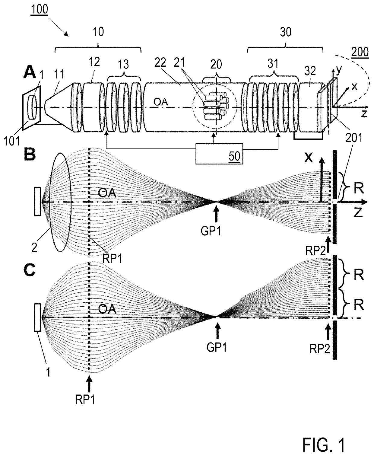
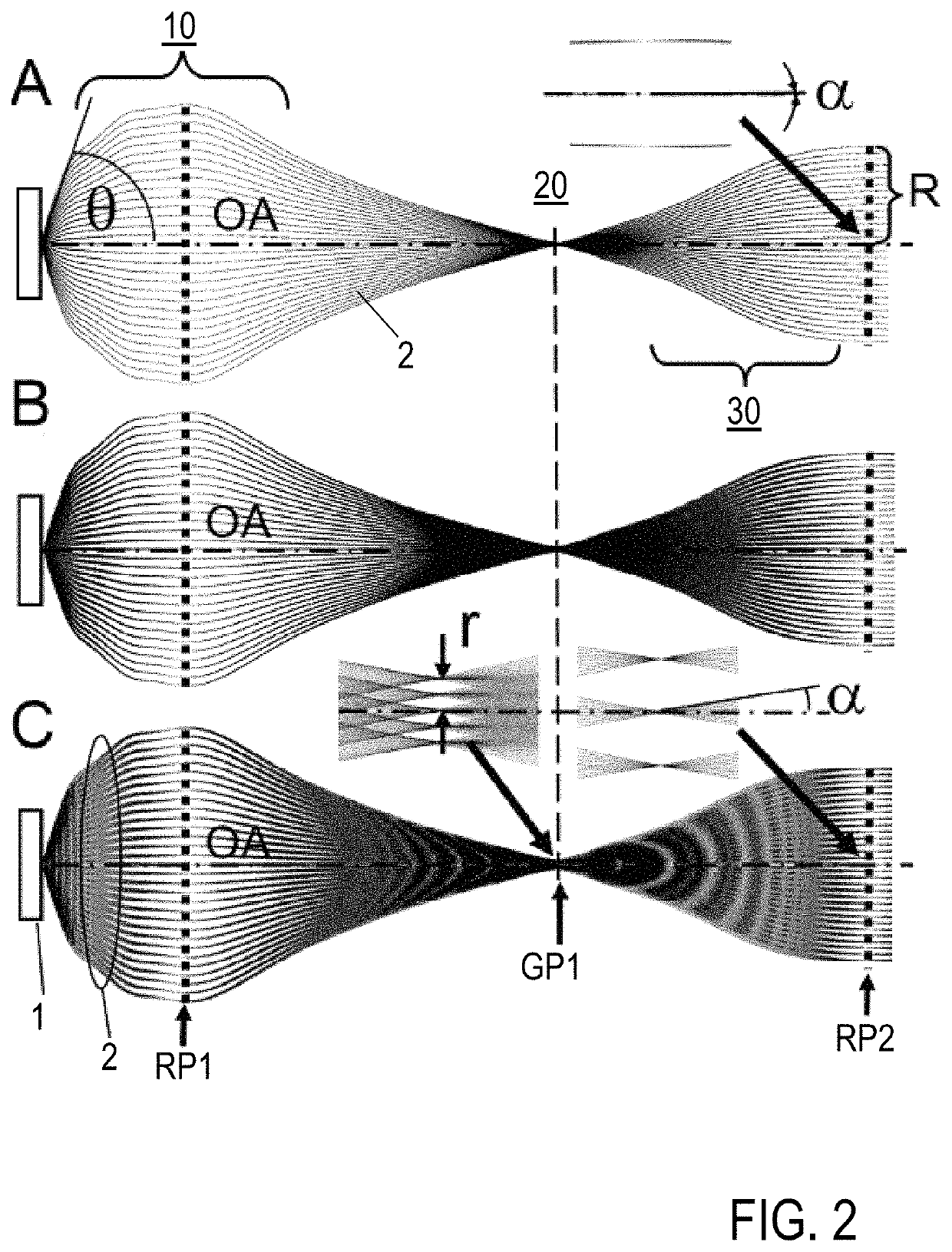
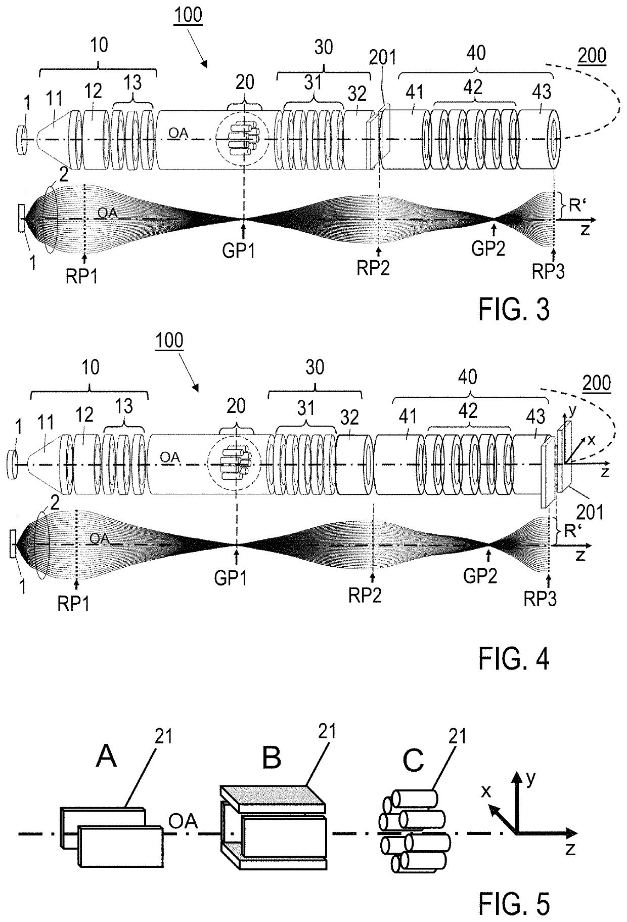
[0064]The invention is described below with exemplary reference to an electron imaging apparatus in combination with a hemispherical analyzer. The invention is not limited to the use of the hemispherical analyzer but is also executable with other types of energy analyzer apparatuses. Details of the excitation of a sample and recording of energy distributions of the electrons emitted from a sample with the hemispherical analyzer are not described, since these are known per se from conventional techniques. The illustrations of the electron-optical components in the drawings are schematic illustrations. Details such as e.g. the arrangement of the electron-optical components in an evacuated space or the formation of electron-optical lenses from spaced lens elements, are not shown. In general, e.g. electron-optical lenses and the associated control circuits can be the same as those essentially known from conventional transfer optics.

[0065]The Figures are described with reference to the r...


PUM


Abstract

An electron imaging apparatus 100 is disclosed, which is configured for an electron transfer along an electron-optical axis OA of an electron 2 emitting sample 1 to an energy analyzer apparatus 200, and comprises a sample-side first lens group 10, an analyzer-side second lens group 30 and a deflector device 20, configured to deflect the electrons 2 in an exit plane of the electron imaging apparatus 100 in a deflection direction perpendicular to the electron-optical axis OA. An electron spectrometer apparatus, an electron transfer method and an electron spectrometry method are also described.

Description

CROSS-REFERENCE TO RELATED APPLICATIONS[0001]This application claims priority to DE 10 2019 107 327.8, filed Mar. 21, 2019, the contents of which are incorporated herein by reference in their entireties for all purposeFIELD OF THE INVENTION[0002]The invention relates to an electron imaging apparatus and an electron transfer method for transferring electrons from a sample to an energy analyzer apparatus, in particular for momentum- and energy-resolved detection of electrons, such as e.g. photoelectrons. The invention further relates to an electron spectrometer apparatus that is provided with the electron imaging apparatus, and an electron spectrometry method. Applications of the invention lie in the electron spectroscopic analysis of samples.BACKGROUND OF THE INVENTION[0003]In the present description, reference is made to the following prior art documents, which illustrate the technical background to the invention:[0004][1] B. Wannberg in “Nucl. Instrum. Meth. A” 601 (2009) 182;[0005...

Claims


Application Information

Patent Timeline
Patent Type & Authority Patents(United States)
IPC IPC(8): H01J49/00H01J49/06H01J49/46H01J37/05H01J37/04H01J37/147H01J37/09H01J37/10
CPCH01J49/06H01J37/04H01J37/05H01J37/09H01J37/10H01J37/147H01J49/46H01J2237/24485H01J49/0031H01J49/48G01N23/227H01J49/44H01J37/252H01J49/484H01J49/0004H01J49/061
Inventor SCHOENHENSE, GERDKAMPEN, THORSTENMAEHL, SVENSCHAFF, OLIVER
Owner SPECS SURFACE NANO ANALYSIS
Why Eureka
Try Eureka