
Device and method of optical range imaging

a technology of optical range imaging and optical range, applied in measurement devices, using reradiation, instruments, etc., can solve the problems of lack of dynamic imaging flexibility in the prior art, relative unreliability of rotating or resonant mechanical elements, and cost, size, weight,

Active Publication Date: 2022-06-21
AAC OPTICS SOLUTIONS PTE LTD
View PDF11 Cites 0 Cited by
  • Summary
  • Abstract
  • Description
  • Claims
  • Application Information

AI Technical Summary

Benefits of technology

[0005]Embodiments of this invention for 3D optical range imaging overcome the weaknesses of prior art. In particular, embodiments permit scanning segments of a field of view in an arbitrary order, and with variable light integration time. This avoids wasting a large fraction of total scan time or a large fraction of a total field of view, when only a portion of a field of view is currently interesting. A first technological problem to solve is lack of dynamic imaging flexibility in the prior art. A second technological problem to solve is the cost, size, weight, and relative unreliability of rotating or resonant mechanical elements. Imaging only selected portions of a total FOV provides faster image update rate than prior art.
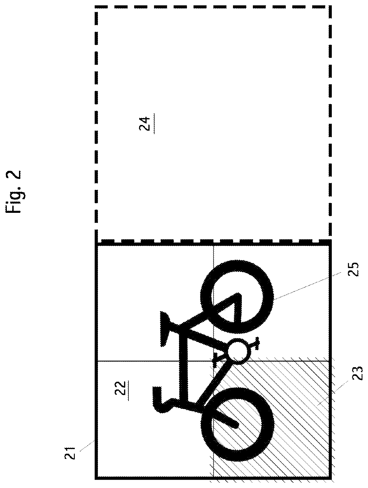
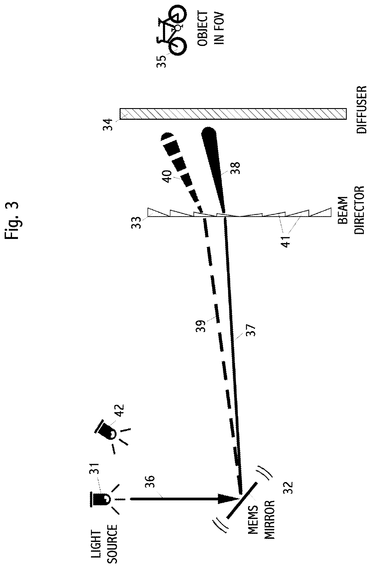
[0010]The non-resonant, one-axis or two-axis MEMs mirror operates in a “step and stare” mode, where each of the P positions is selected by a controller in any arbitrary order. The mirror is moved to a selected pair of angles (one for each axis of rotation of the mirror), and then held fixed. Light from the modulated light source reflects off the mirror, through one of P portions of a beam director, such as a prism array of P prisms, through a diffuser, and finally out of the device. A beam director may also be called a, “directional lensing element” or elements. The beam director directs a light beam to one of P beam directions, or beam direction angles. The light illuminates an illumination reduced field of view of the whole target FOV. Light from objects in this selected illumination reduced field of view reflects back to the device, where it is focused by one of N focus lenses to its associated one of N image sensor chips. A portion of that image sensor then integrates reflected light for a selected amount of time, which may be dynamically selectable. Then, the mirror moves (“steps”) to a next position, illuminating (“stare”) another reduced field of view. This continues, until all 16 (P=16 in this example) reduced fields of view are illuminated and imaged. Then, the process repeats. A novel aspect of this embodiment is that the reduced fields of view, “segments” (also called regions) of the total FOV, may be illuminated and imaged in any arbitrary order. This permits portions of the total FOV to be selected for either more frequent imaging or longer time-period imaging. For example, a region of interest might be imaged 60 times per second, while the total target FOV is imaged completely only 15 times per second. As another example, distant or dim objects may use a longer integration time than near objects. The frequency or signal shape of the modulator signal may be changed to provide a different, or larger, total distance dynamic range of an embodiment, or to improve the signal-to-noise ratio of received signals.
[0013]Typically, image sensor chips operate either in an “integration” mode, wherein all the individual pixel light sensors integrate light, or in a “read out” mode where data in the chip is read out. Typically, the chip operates alternately and repetitively between these two modes. However, read out time can be significant. Thus, a single chip is not able to be integrating light full time. A key feature of embodiments is the use of multiple, N, image sensor chips, where while one chip is integrating light, one or more of the other chips is reading out data. In this way, some portion of the total FOV is being illuminated and imaged, avoiding the “dead time” of single-sensor prior art. Other operating modes and sequences are possible, and those described herein are non-limiting. In particularly, pixels may be combined into groups, pixels or associated electronics may be arranged in rows or other portions of a chip that may operate independently or with different operating parameters.

Problems solved by technology

A first technological problem to solve is lack of dynamic imaging flexibility in the prior art.
A second technological problem to solve is the cost, size, weight, and relative unreliability of rotating or resonant mechanical elements.

Method used


Image

  • Device and method of optical range imaging
  • Device and method of optical range imaging
  • Device and method of optical range imaging

Examples


Embodiment Construction

[0024]Scenarios, options and examples are non-limiting embodiments.

[0025]The exact acronym for LIDAR varies in the art. It may be Laser Detection And Ranging; Light Detection And Ranging; LIght Detection And Ranging; a combination of the words light and radar. Our usage herein is LIght Detection And Ranging; however the exact acronym is non-limiting. Other terms for LIDAR include, “3D optical ranging.”

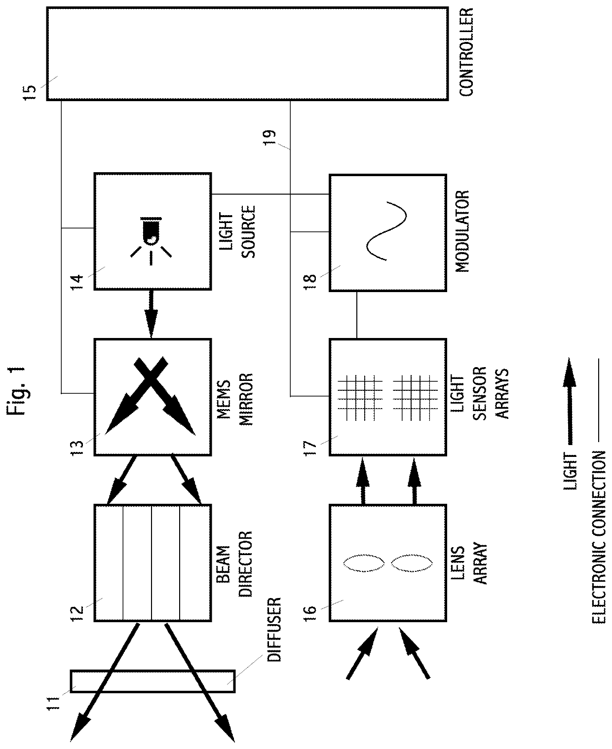
[0026]Turning first to FIG. 1, we see a schematic of major elements in an embodiment. The upper half of the Figure is primarily elements in the illumination subsystem and the lower half of the Figure is primarily elements in the imaging subsystem. To the right is a controller comprising control electronics, such as a processor, data and program memory, input / output interfaces, power supplies, and the like. 14 shows a continuous wave, modulated light source such as one or more LEDs, solid-state lasers, or other modulated light sources. A modulated light source may use an amplitude modul...


PUM


Abstract

An optical device creates 3D images comprising a field of points, each point comprising horizontal, vertical, and distance metrics. The device comprises an illumination subsystem, comprising light sources, such as LEDs, a non-resonant beam steering element such as a micro-electro-mechanical system (MEMs) mirror, beam-shaping optics, a beam director plate, and a diffuser. The device also comprises an imaging subsystem with one or more optical detector chips that measure time-of-flight (TOF). Devices may dynamically and sequentially images solid-angle sub-regions of interest, in an arbitrary order, out of a total FOV, using eye-safe illumination. The corresponding received image portions are stitched together. The beam steering element is non-resonant, allowing arbitrary and rapid changes to its pointing vector. Beam shaping optics generates rectangular solid-angle illumination. One detector chip integrates light from one sub-region while another chip is reads out image data.

Description

PRIORITY[0001]This application claims priority to U.S. Provisional Application No. 62 / 688,165, filed 21 Jun. 2018.FIELD OF THE INVENTION[0002]This invention is in the field of optical, wide field of view, “3D imaging” ranging devices such as scanning LIDAR.BACKGROUND OF THE INVENTION[0003]Devices such as LIDAR are useful for autonomous vehicles and other applications to create a, digital, three-dimensional (3D) representation of objects within a field of view (FOV). LIDARs may be used by autonomous vehicles to find, and then quickly identify, nearby objects. They have numerous other applications, including safety, construction, and mapping. Prior art LIDARs use high-intensity, sharply pulsed parallel laser beams or FMCW (Frequency Modulated Continuous Wave) modulated beams, which are continuously scanned. This scanning is done either by rotation around a mechanical axis or by light reflection off spinning or resonantly vibrating mirrors. Alternatively, prior art devices use high int...

Claims


Application Information

Patent Timeline
Patent Type & Authority Patents(United States)
IPC IPC(8): G01S17/894G01S7/481G01S7/4863
CPCG01S17/894G01S7/4816G01S7/4817G01S7/4863G01S17/931
Inventor SPICKERMANN, RALPHKALLURI, SRINATHJAIN, SIDDHARTH
Owner AAC OPTICS SOLUTIONS PTE LTD
Learn More