Semiconductor package structure with landing pads and manufacturing method thereof

a technology of semiconductors and packaging, applied in the direction of semiconductor devices, semiconductor/solid-state device details, electrical apparatus, etc., can solve the problems of reducing reducing the landing area provided by the foregoing method, etc., to improve the reliability and yield rate of the overall semiconductor package structure, expand the landing area of the landing pad, and enhance the bonding strength

Active Publication Date: 2022-09-06
POWERTECH TECHNOLOGY INC
View PDF6 Cites 0 Cited by
  • Summary
  • Abstract
  • Description
  • Claims
  • Application Information

AI Technical Summary

Benefits of technology

[0004]The disclosure provides a semiconductor package structure and a method of manufacturing the same, which can effectively expand the landing area of the landing pad and enhance the bonding strength for the landing pad and the elements disposed thereon, thereby improving the reliability and yield rate of the overall semiconductor package structure.
[0007]Based on the above, in the disclosure, since the first redistribution layer includes at least one conductive pattern and at least one dielectric layer stacked on each other, wherein the conductive pattern includes a plurality of landing pads, and each of the landing pads is separated from the dielectric layer, the bonding strength for the landing pad and the element disposed thereon (such as conductive connectors) can be enhanced, thereby improving the reliability and yield rate of the overall semiconductor package structure.

Problems solved by technology

However, with the miniaturization of the semiconductor package structure, the landing area provided by the foregoing method is also reduced, which causes the problem of insufficient bonding strength for the landing pad and the elements disposed thereon, and may reduce the reliability and yield rate of the overall semiconductor package structure.
Therefore, it has become a challenge to find out how to effectively expand the landing area of the landing pad and enhance the bonding strength for the landing pad and the elements disposed on the landing pad, thereby improving the reliability and yield rate of the overall semiconductor package structure.

Method used


Image

  • Semiconductor package structure with landing pads and manufacturing method thereof
  • Semiconductor package structure with landing pads and manufacturing method thereof
  • Semiconductor package structure with landing pads and manufacturing method thereof

Examples


Embodiment Construction

[0013]Directional terms used herein (e.g., up, down, right, left, front, back, top, bottom) are used only as a reference to the drawing and are not intended to imply specific orientation.

[0014]Unless explicitly described, any method described herein is by no means intended to be interpreted as requiring that its steps be performed in a particular order.

[0015]The disclosure is described more thoroughly with reference to the drawings of the present embodiment. However, the disclosure can also be embodied in various forms, and should not be limited to the embodiments described herein. The thickness, dimension or size of layers or regions in the drawings are exaggerated for clarity. The same or similar reference numbers denote the same or similar elements, and the above content will not be repeated in the following paragraphs.

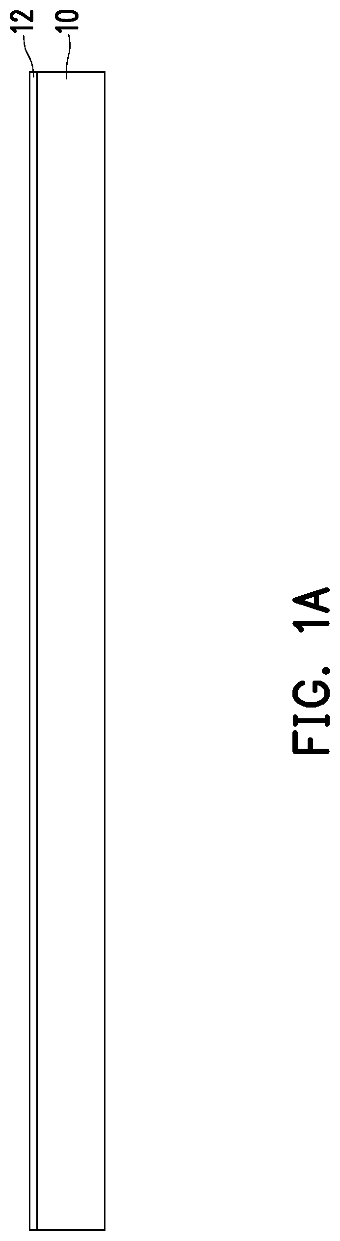
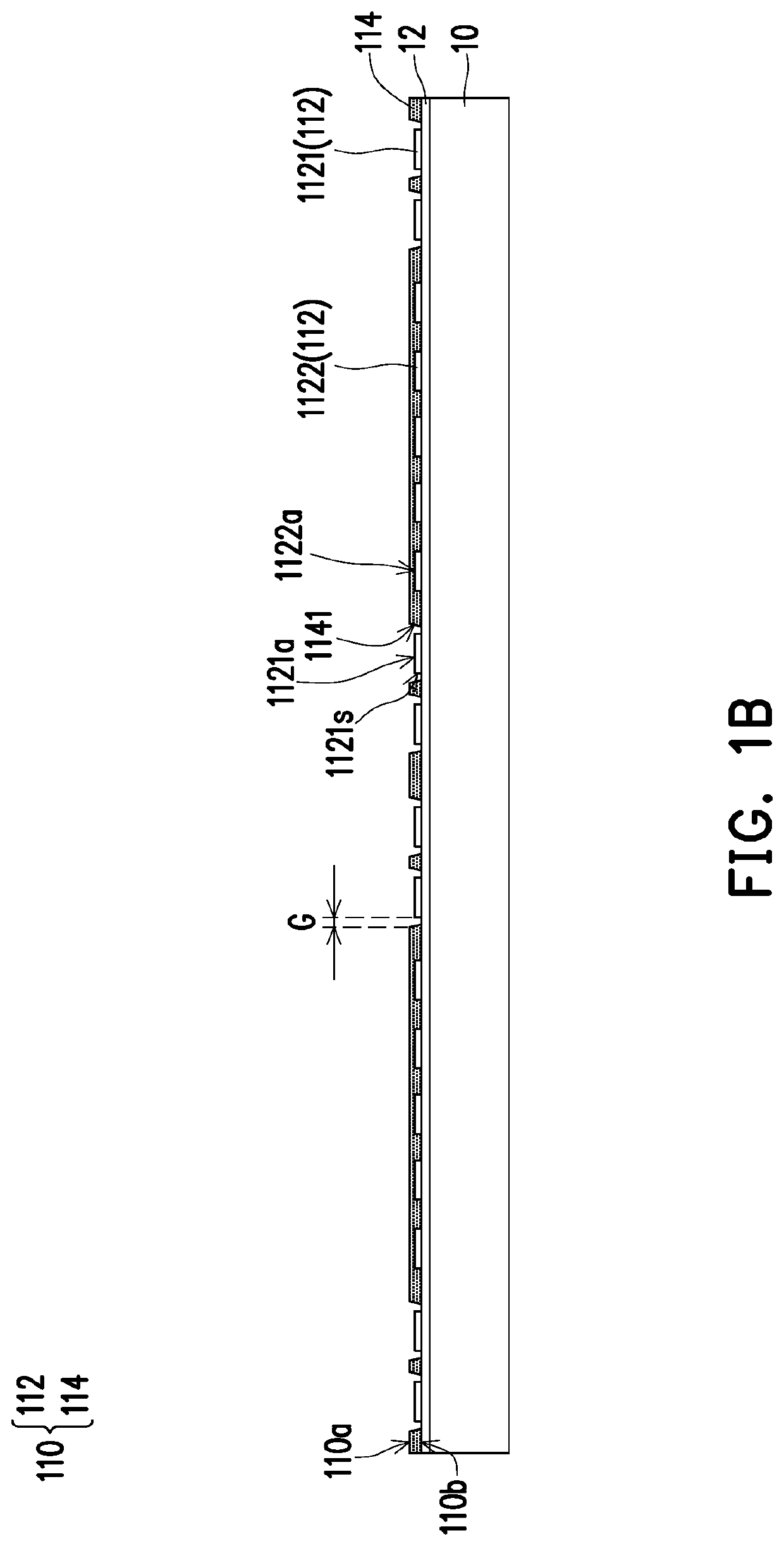
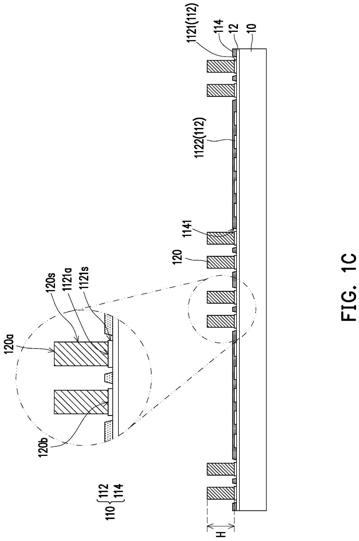
[0016]FIG. 1A to FIG. 1I are partial schematic cross-sectional views of a part of manufacturing method for semiconductor package structure according to an embodime...


PUM

PropertyMeasurementUnit
heightaaaaaaaaaa
heightaaaaaaaaaa
heightaaaaaaaaaa

Abstract

A semiconductor package structure includes a first redistribution layer, a plurality of conductive connectors, a chip, and an encapsulant. The first redistribution layer has a first surface and a second surface opposite to the first surface. The first redistribution layer includes at least one conductive pattern and at least one dielectric layer stacked on each other. The conductive pattern includes a plurality of landing pads, and each of the landing pads is separated from the dielectric layer. The conductive connectors are located on the first surface. Each of the conductive connectors is corresponding to and electrically connected to one of the landing pads. The chip is located on the first surface. The chip is electrically connected to the first redistribution layer. The encapsulant encapsulates the chip and the conductive connectors. A manufacturing method of a semiconductor package structure is also provided.

Description

CROSS-REFERENCE TO RELATED APPLICATION[0001]This application claims the priority benefit of Taiwan application no. 109114563, filed on Apr. 30, 2020. The entirety of the above-mentioned patent application is hereby incorporated by reference herein and made a part of this specification.BACKGROUNDField of the Disclosure[0002]The disclosure relates to a package structure and a manufacturing method thereof, and particularly to a semiconductor package structure and a manufacturing method thereof.Description of Related Art[0003]Generally speaking, in the redistribution layer of the current semiconductor package structure, a landing pad for electrical connection with other elements usually exposes a part of the top surface as a landing area. However, with the miniaturization of the semiconductor package structure, the landing area provided by the foregoing method is also reduced, which causes the problem of insufficient bonding strength for the landing pad and the elements disposed thereon...

Claims


Application Information

Patent Timeline
Patent Type & Authority Patents(United States)
IPC IPC(8): H01L23/00H01L23/31H01L21/48H01L21/56
CPCH01L24/25H01L21/4803H01L21/4846H01L21/561H01L23/3128H01L24/24H01L24/82H01L2224/2402H01L2224/24011H01L2224/24175H01L2224/2518H01L2224/82005H01L23/5389H01L23/49816H01L21/6835H01L2221/68345H01L2221/68359H01L2224/18H01L24/19
Inventor WANG, JEFFREYHUANG, JEN-IHUANG, KUN-YUNG
Owner POWERTECH TECHNOLOGY INC
Why Eureka
Try Eureka