Interfacial layer for high resolution lithography (HRL) and high speed input/output (IO or I/O) architectures

a high-resolution lithography and interfacial layer technology, applied in the direction of photomechanical equipment, insulating substrate metal adhesion improvement, instruments, etc., can solve the problems of unwanted surface reflection of the hieb, the creation of unwanted surface reflection off one or more layers exposed to a beam of electrons, and the pressure to reduce the fls

Active Publication Date: 2022-09-13
INTEL CORP
View PDF5 Cites 0 Cited by
  • Summary
  • Abstract
  • Description
  • Claims
  • Application Information

AI Technical Summary

Problems solved by technology

Currently, semiconductor packaging, semiconductor fabrication, and / or PCB fabrication technologies face pressures to decrease the FLS.
One drawback of using an HRL technique to fabricate interconnects and / or features is the creation of unwanted surface reflection off one or more layers exposed to a beam of electrons (e.g., an HIEB, etc.).
However, maintaining the fidelity can result in unwanted surface reflection of the HIEB off a resist layer that is close to a metal layer.
A reflected exposure beam also retains its fidelity, however, this fidelity is unwanted due to its effect of decreasing the sharpness of features, especially when those features are close to the metal surface by curing the resist materials.
The unwanted surface reflection described above can negatively affect an ability of an beam of electrons to define dense fine line space features close to a metal layer (e.g., a seed layer, etc.).
This requires thick electroless or physical vapor deposition / chemical vapor deposition (PVD / CVD)”, which can limit manufacturing options and be a showstopper for most packaging architectures.
Also, thick metal layers can limit the benefits of HRL due to the thick seed removal requirements.
Current OAP formulations, however, have limited properties, which can in turn limit their use in HRL.

Method used


Image

  • Interfacial layer for high resolution lithography (HRL) and high speed input/output (IO or I/O) architectures
  • Interfacial layer for high resolution lithography (HRL) and high speed input/output (IO or I/O) architectures
  • Interfacial layer for high resolution lithography (HRL) and high speed input/output (IO or I/O) architectures

Examples


Embodiment Construction

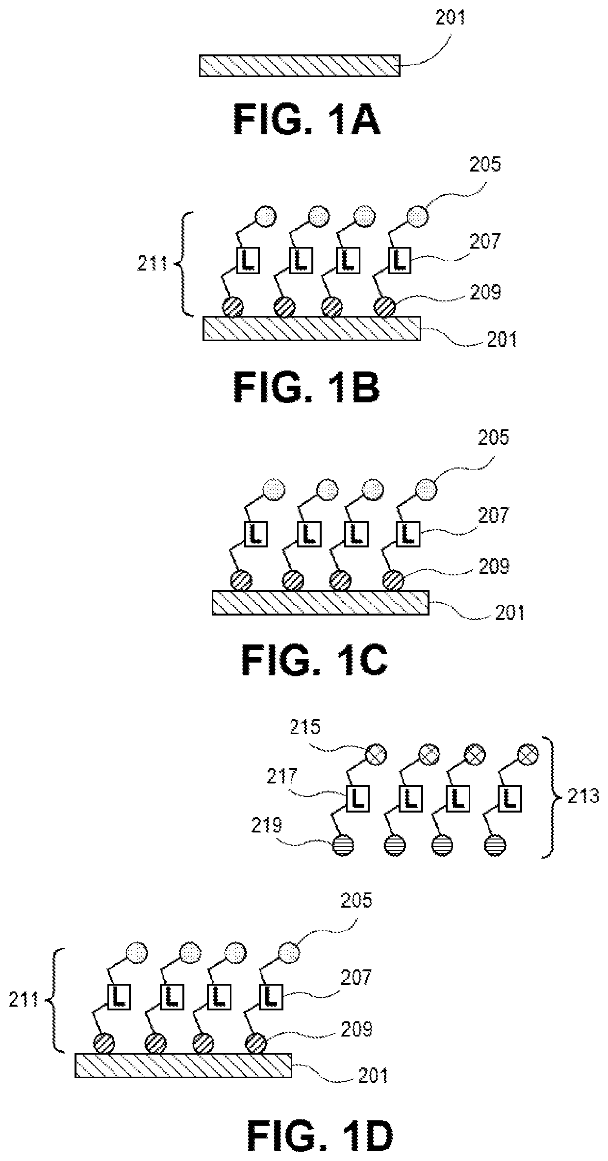
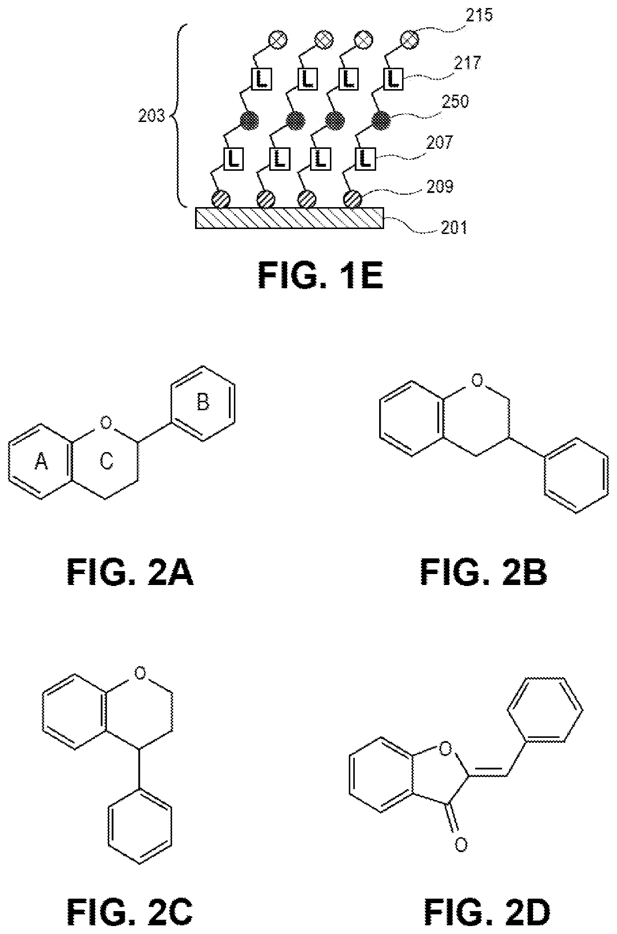
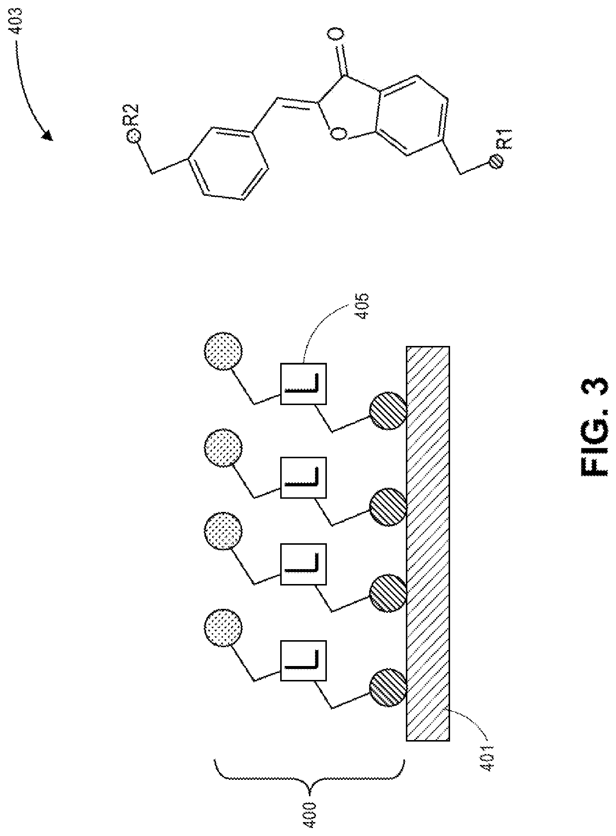
[0019]Embodiments described herein provide techniques for forming an interfacial layer on a metal layer to assist with improving adhesion of a resist layer to the metal layer and with improving use of one or more lithography techniques (e.g., an HRL, any other lithography technique known in the art, any combination of lithography techniques known in the art, etc.) to fabricate interconnects and / or features using the resist and metal layers for a package substrate, a semiconductor package, or a PCB. For one embodiment, the interfacial layer includes, but is not limited to, an organic interfacial layer. Examples of organic interfacial layers include, but are not limited to, self-assembled monolayers (SAMs), constructs and / or variations of SAMs, organic adhesion promotor moieties, and non-adhesion promoter moieties. The interfacial layer can be in film form and / or any other suitable form known in the art. For one embodiment, when the interfacial layer comprises an SAM, the SAM is forme...


PUM

PropertyMeasurementUnit
wavelengthsaaaaaaaaaa

Abstract

Embodiments described herein are directed to interfacial layers and techniques of forming such interfacial layers. An interfacial layer having one or more light absorbing molecules is on a metal layer. The light absorbing molecule(s) may comprise a moiety exhibiting light absorbing properties. The interfacial layer can assist with improving adhesion of a resist layer to the metal layer and with improving use of one or more lithography techniques to fabricate interconnects and / or features using the resist and metal layers for a package substrate, a semiconductor package, or a PCB. For one embodiment, the interfacial layer includes, but is not limited to, an organic interfacial layer. Examples of organic interfacial layers include, but are not limited to, self-assembled monolayers (SAMs), constructs and / or variations of SAMs, organic adhesion promotor moieties, and non-adhesion promoter moieties.

Description

BACKGROUNDField[0001]Embodiments described herein generally relate to package substrates, semiconductor packages, or printed circuit boards (“PCB”). More particularly, but not exclusively, embodiments described herein relate to an interfacial layer that is on or part of a package substrate, a semiconductor package, and / or a PCB.Background Information[0002]A package substrate, a semiconductor package, or a PCB may comprise one or more layers, where at least one of the layers comprises one or more features formed therein or thereon. A semiconductor package may comprise a package substrate and one or more semiconductor dies (which may also be referred to as integrated circuits (ICs) herein) on the package substrate. Also, a semiconductor package may be on a PCB.[0003]Examples of layers include, but are not limited to, one or more of: (i) a metal layer; (ii) a dielectric layer; (iii) a resist layer; (iv) any other layer known in the art of semiconductor packaging, the art of semiconduct...

Claims


Application Information

Patent Timeline
Patent Type & Authority Patents(United States)
IPC IPC(8): H05K3/38H01L21/027H01L21/48H05K1/03H01L23/498H01L23/00
CPCH05K3/386H01L21/0273H01L21/4846H01L23/49894H05K1/0353H01L24/16H01L2224/16225H01L21/321H01L21/0276G03F7/091G03F7/165H01L2224/16227H01L2924/15311H01L2224/131H01L2223/6627H01L2223/6638H01L2924/014H01L2924/00014
Inventor NAD, SUDDHASATTWAMANEPALLI, RAHULWALL, MARCEL
Owner INTEL CORP
Why Eureka
Try Eureka