Unlock instant, AI-driven research and patent intelligence for your innovation.

Output stage circuit

a technology of output stage and output circuit, which is applied in the direction of amplifier details, multiple input and output pulse circuits, amplifiers with only semiconductor devices, etc., can solve the problems of reducing the service life or even directly burning out parts of the output stage circuit or other circuits, so as to shorten the service life

Active Publication Date: 2022-09-20
VIA ALLIANCE SEMICON CO LTD
View PDF3 Cites 1 Cited by
  • Summary
  • Abstract
  • Description
  • Claims
  • Application Information

AI Technical Summary

Benefits of technology

The invention is an output stage circuit that dynamically adjusts a bias voltage based on the output voltage to prevent damage to the circuit due to overvoltage. By adjusting the bias voltage, the circuit ensures that the three-terminal voltages of each transistor do not exceed the withstand voltage of the transistor, reducing the risk of damage and extending the lifespan of the circuit. The output stage circuit is implemented by an amplifier circuit structure of at least three tiers and a floating bias voltage.

Problems solved by technology

However, when the output stage circuit is actually used, since there must be a phenomenon of voltage overshoot of the input / output signal, the withstand voltages of some components of the output stage circuit may exceed designed predetermined values, which reduces a service life of the output stage circuit, or even directly burns out a part of components of the output stage circuit or other circuits.

Method used


Image

  • Output stage circuit
  • Output stage circuit
  • Output stage circuit

Examples


Embodiment Construction

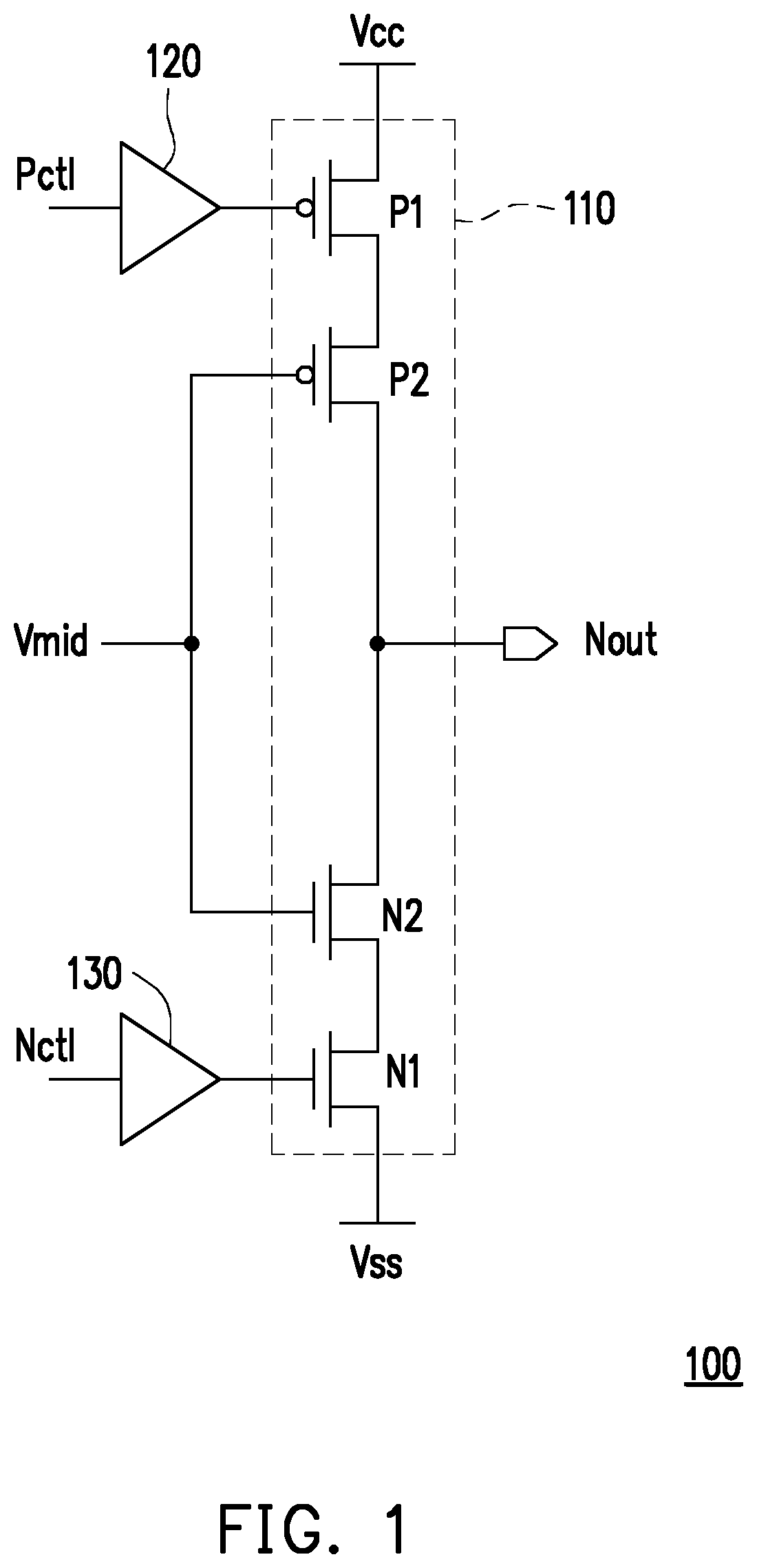
[0015]FIG. 1 is a circuit diagram of an output stage circuit 100. The output stage circuit 100 in FIG. 1 comprises a two-tier amplifier circuit 110 composed of transistors P1, P2, N1 and N2, and two pre-drivers 120 and 130. It is assumed that a withstand voltage of each transistor of the output stage circuit 100 is 1.8V due to limitation of a semiconductor process, and a chip using the output stage circuit 100 needs to transmit a data signal with a maximum voltage of 3.3V at an output terminal Nout of the output stage circuit 100 due to a transmission protocol of a specific interface. The transistors P1 and P2 of the embodiment are both P-type metal-oxide-semiconductor field-effect transistors (MOSFETs), and the transistors N1 and N2 are both N-type MOSFETs.

[0016]The pre-driver 120 receives a first control signal Pctl and pre-drives the first control signal Pctl, and transmits the pre-driven first control signal Pctl to a control terminal (a gate) of the transistor P1. The pre-drive...


PUM


Abstract

An output stage circuit comprising a bias voltage generator, a first amplifier circuit and a second amplifier circuit is provided. The bias voltage generator is coupled to an output terminal of the output stage circuit to generate a bias voltage according to an output voltage of the output terminal. The first amplifier circuit is coupled to the output terminal, a first power supply terminal and the bias voltage generator, receives a first pre-driving signal, a first predetermined voltage and the bias voltage, and determines whether to transmit a first voltage to serve as the output voltage. The second amplifier circuit is coupled to the output terminal, a second power supply terminal and the bias voltage generator, receives a second pre-driving signal, a second predetermined voltage and the bias voltage, and determines whether to transmit a second voltage to serve as the output voltage.

Description

CROSS-REFERENCE TO RELATED APPLICATION[0001]This application claims the priority benefit of China application no. 202010278121.8, filed on Apr. 10, 2020. The entirety of the above-mentioned patent application is hereby incorporated by reference herein and made a part of this specification.BACKGROUNDTechnical Field[0002]The disclosure relates to an output stage circuit, and particularly relates to an output stage circuit capable of avoiding or reducing damage resulting from voltage overshoot.Description of Related Art[0003]When the structure of a chip is designed, characteristics of manufactured components may be different due to different semiconductor processes. For example, transistors produced by different semiconductor processes may have different voltage withstand levels. In addition, based on technical specifications and application limitations and advances in semiconductor technology, an input / output signal voltage used in a currently circuit is designed in accordance with ru...

Claims


Application Information

Patent Timeline
Patent Type & Authority Patents(United States)
IPC IPC(8): H03F3/16H03K5/24
CPCH03F3/16H03K5/24H03F1/523H03F3/68H03F3/2173H03F1/0272
Inventor LI, SHENLIU, ZHONGDING
Owner VIA ALLIANCE SEMICON CO LTD