Electrostatic holding apparatus with a layered composite electrode device and method for the production thereof

a technology of composite electrodes and holding apparatuses, applied in the field of holding apparatuses, can solve the problems of increasing production effort, high cost, and requiring regular cycle renewal, and achieve the effects of simple connection to the base body, limited chemical and/or physical resistance, and complex time-consuming processing

Active Publication Date: 2022-11-22
ASML NETHERLANDS BV
View PDF19 Cites 0 Cited by
  • Summary
  • Abstract
  • Description
  • Claims
  • Application Information

AI Technical Summary

Benefits of technology

[0007]In US 2015 / 0348816 A1, an apparatus according to the aforementioned first variant of electrostatic clamps is described. Herein, a dielectric disk coated with an electrode is adhesively bonded over the full area onto a base body. The adhesive is selected such that, apart from its adhesive properties, it also serves as an insulator between the base body and the electrode. The burls support plane is introduced into the dielectric in the device described in US 2015 / 0348816 A1. In this apparatus, the full-area adhesive bonding of the dielectric disk, whereby the adhesive is also situated under the individual burls, can have disadvantageous effects. A shrinking or ageing of the adhesive polymer can lead to a position change of the burls in the z-direction and thus disadvantageously change the evenness on the clamp support area. Furthermore, in US 2015 / 0348816 A1, it is described that the adhesive evens out unevennesses between the dielectric and the base body. This can have the result, however, that under the individual burls, different adhesive layer thicknesses occur and thus the compressibility of the individual burls varies, which can also have an effect on the evenness of the support area during later operation of the device and the action of a clamping pressure.
[0008]A holding apparatus according to the aforementioned second variant of electrostatic clamps wherein the electrode device is not integrated into the base body, but is arranged on its surface between the burls (burl bottom) is described, for example, in US 2009 / 0079525 A1 and in US 2013 / 0308116 A1. In this case, the electrode device comprises a layered structure between adjacent burls with a bottom plastics insulating layer, in the upper side of which the electrodes are integrated, and a dielectric layer made of a plastics or glass, which extends over the insulating layer with the electrode. This configuration represents a suggestion for the arrangement of the electrodes between the burls, although no methods are disclosed as to how the layered structure is to be produced on a holding apparatus for practical applications with, for example, several thousand burls. In particular, it is disadvantageous, that no setting of the distance of the electrodes from the burls support plane or of the gap spacing is provided, so that the electrostatic clamping pressure can vary over the area of the holding apparatus.
[0009]From U.S. Pat. No. 9,673,079 B1, it is known, for the production of an electrostatic holding apparatus, to provide the electrode device as a separate component with a self-supporting silicon plate, electrode layers on the silicon plate and a covering SiN dielectric layer. The silicon plate has holes for receiving the burls of the base body. For the connection of the electrode device to the base body, the silicon plate is adhesively bonded onto the base body, wherein the burls protrude through the holes of the electrode device. With this method, particular advantages arise from the separate production of the electrode device and its simple connection to the base body. It can, however, be disadvantageous that, for example, through thickness variations in the adhesive connection between the electrode device and the base body, variations of the gap spacing can arise above the electrode device. Furthermore, it is required that the silicon plate is as thin as possible or the burl height is as great as possible, which leads to a complex time-consuming processing.
[0010]According to US 2012 / 0274920 A1, it is proposed to produce the electrode device with thin film technology in the spacings between the burls. Firstly, a planarization layer is formed on the base body between the burls, on which a polymer or SiOx-based insulator layer, the electrode layer and a polymer or SiOx-based dielectric layer are deposited. With this technology, the planarization layer permits a planarizing of the electrode device. It is disadvantageous, however, that even in this case, through variations in the thin-film deposition, variations of the gap spacing and thus of the electrostatic clamping pressure arise. Furthermore, the thin layers are sensitive to damage on use of the holding apparatus.
[0011]In order to prevent variations of the gap spacing, it is proposed in US 2018 / 0047605 A1 to form the electrode device in the spaces between the burls by means of a polymer-based insulator layer, electrode layers on the insulator layer and a covering polymer-based dielectric layer. Variations of the gap spacing should be excluded in that the upper sides of the insulating and dielectric layers are adjusted before their hardening, in each case, with a reference tool. With this technology, variations of the holding forces through variations of the gap spacing are prevented. A disadvantage arises, however, from the large number of successive operations to be carried out in the production of the holding apparatus. A further more important disadvantage results from the use of polymers for the formation of the insulator and dielectric layers. Polymer plastics have a limited chemical and / or physical resistance under the conditions of use of electrostatic holding apparatuses, in particular in the processing of semiconductor wafers. Unwanted substances can be released and / or ageing processes of the polymers can restrict the working life of the holding apparatus.
[0012]In the German patent application DE 10 2018 116 463.7 (not yet published at the priority date of the present specification), a further method for producing a holding apparatus according to the above second variant is described. Thereby, an electrode device is produced in that a dielectric disk which carries an electrode layer is adhesively bonded onto the upper side of the base body and is subsequently thinned for setting the thickness of the finished dielectric layer and the gap spacing between the burls support plane and the upper side of the dielectric layer. This method advantageously enables the setting of a desired gap spacing. However, since the adhesive forms the insulator layer between the electrode layer and the base body, disadvantages can arise with regard to the reliability of the electrical insulation. For example, inhomogeneities in the adhesive, for example particles, can impair the dielectric strength of the insulator layer.

Problems solved by technology

In this case, additional wear prevention layers are required which increase the production effort and require renewal in regular cycles.
However, the complex multilayered structure of the electrode device has previously been associated with a long, almost entirely serial process chain with high costs, a restricted yield, a high degree of effort and high costs due to post-processing in the production, and with long delivery times.
In this apparatus, the full-area adhesive bonding of the dielectric disk, whereby the adhesive is also situated under the individual burls, can have disadvantageous effects.
A shrinking or ageing of the adhesive polymer can lead to a position change of the burls in the z-direction and thus disadvantageously change the evenness on the clamp support area.
This can have the result, however, that under the individual burls, different adhesive layer thicknesses occur and thus the compressibility of the individual burls varies, which can also have an effect on the evenness of the support area during later operation of the device and the action of a clamping pressure.
In particular, it is disadvantageous, that no setting of the distance of the electrodes from the burls support plane or of the gap spacing is provided, so that the electrostatic clamping pressure can vary over the area of the holding apparatus.
It can, however, be disadvantageous that, for example, through thickness variations in the adhesive connection between the electrode device and the base body, variations of the gap spacing can arise above the electrode device.
Furthermore, it is required that the silicon plate is as thin as possible or the burl height is as great as possible, which leads to a complex time-consuming processing.
It is disadvantageous, however, that even in this case, through variations in the thin-film deposition, variations of the gap spacing and thus of the electrostatic clamping pressure arise.
Furthermore, the thin layers are sensitive to damage on use of the holding apparatus.
A disadvantage arises, however, from the large number of successive operations to be carried out in the production of the holding apparatus.
A further more important disadvantage results from the use of polymers for the formation of the insulator and dielectric layers.
Polymer plastics have a limited chemical and / or physical resistance under the conditions of use of electrostatic holding apparatuses, in particular in the processing of semiconductor wafers.
Unwanted substances can be released and / or ageing processes of the polymers can restrict the working life of the holding apparatus.
However, since the adhesive forms the insulator layer between the electrode layer and the base body, disadvantages can arise with regard to the reliability of the electrical insulation.
For example, inhomogeneities in the adhesive, for example particles, can impair the dielectric strength of the insulator layer.
Finally, a general disadvantage of conventional holding apparatuses lies therein that the function of the holding apparatus can conventionally only be tested on the finished product in that the electrode device has a working voltage applied to it and the holding force achieved is measured.
In the event of functional errors or insufficient holding force, a correction is typically not possible, so that the holding apparatus must be discarded as a reject.
The problems mentioned occur not only in holding apparatuses for holding semiconductor wafers, but also in other uses, for example, in holding apparatuses for holding glass plates.

Method used


Image

  • Electrostatic holding apparatus with a layered composite electrode device and method for the production thereof
  • Electrostatic holding apparatus with a layered composite electrode device and method for the production thereof
  • Electrostatic holding apparatus with a layered composite electrode device and method for the production thereof

Examples


Embodiment Construction

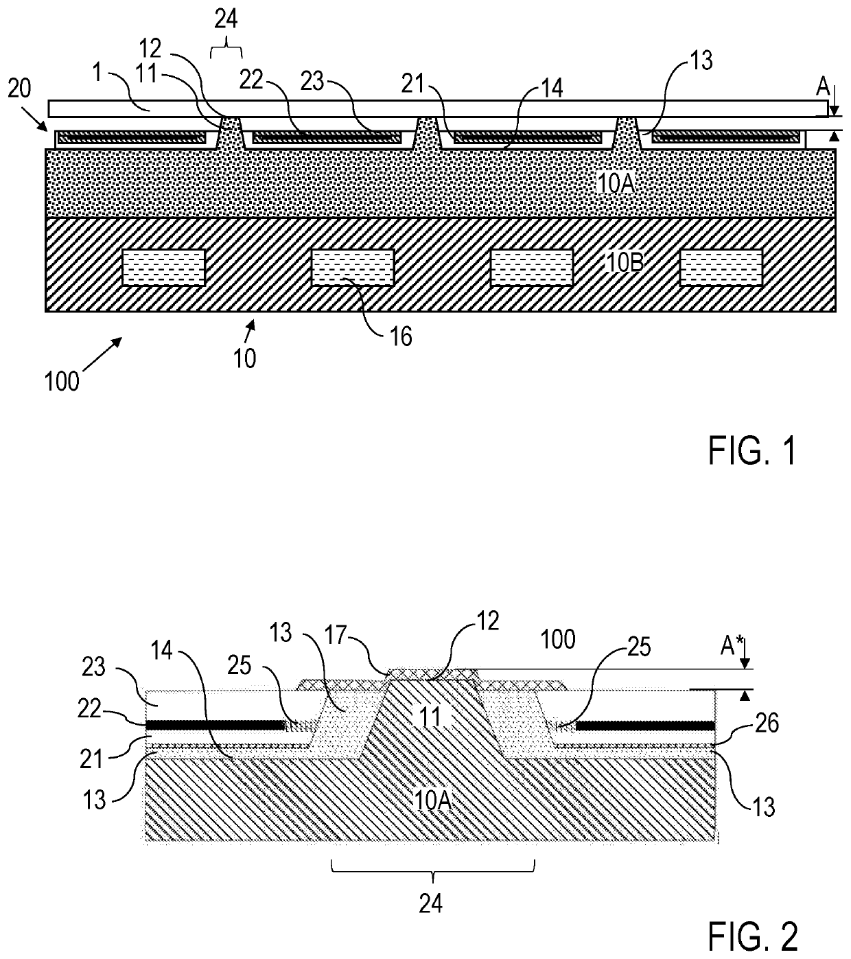
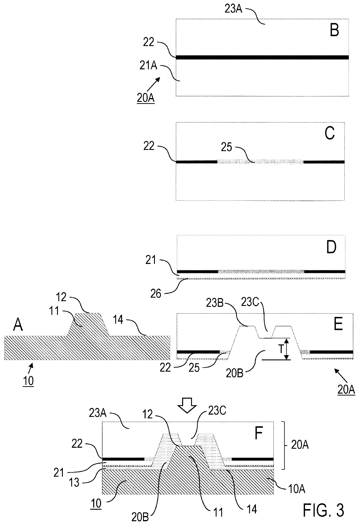
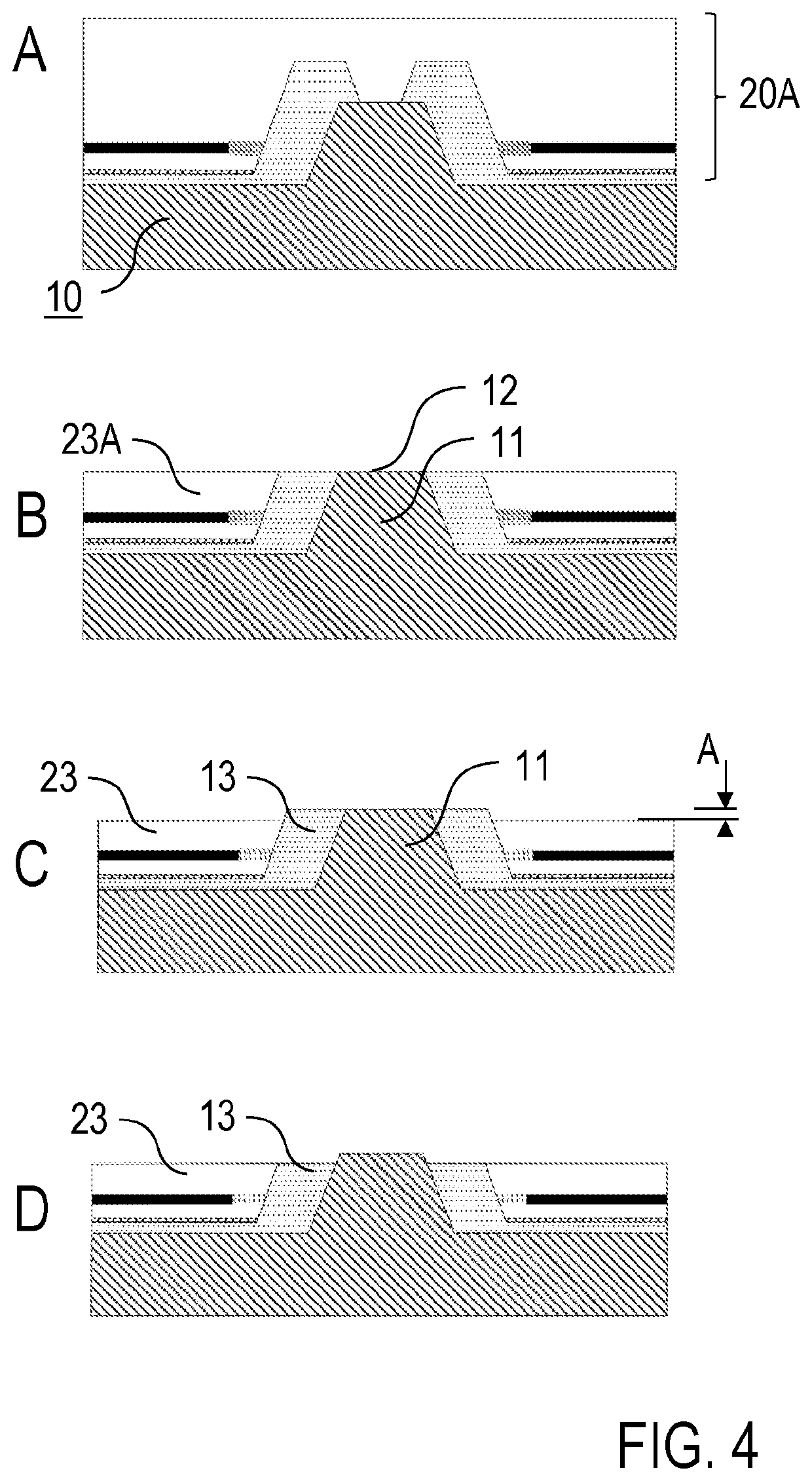
[0052]Preferred embodiments of the invention are described below making exemplary reference to features of an electrostatic holding apparatus for silicon wafers, wherein the electrostatic holding apparatus is shown schematically and not to scale. The implementation of the invention is not restricted to this use. Other uses of the holding apparatus are possible, for example, for the holding of glass plates with metal coatings, or exposure masks, wherein for other uses, the form of the base body, in particular the burls, the materials and the dimensions of the electrode device are adapted to the specific requirements. Deviating from the illustration, the base body can comprise a single plate or can be made multilayered from a plurality of sub-plates. Furthermore, for practical applications of the holding apparatus in the handling of semiconductor wafers, the base body is provided on both sides with burls and each provided with an electrode device. Details of the specific configuration...


PUM

PropertyMeasurementUnit
diameteraaaaaaaaaa
diameteraaaaaaaaaa
heightaaaaaaaaaa

Abstract

Holding apparatus 100 for electrostatic holding component 1 (e.g., semiconductor wafer), includes base body 10 with at least one plate 10A, protruding burls 11 on upper side of plate and end faces 12 of which span a burls support plane for supporting component, and electrode device 20 in layered form in spacings between burls and insulator layer 21 which is connected to plate, dielectric layer 23 of inorganic dielectric and electrode layer 22 between insulator and dielectric layers. Between burls support plane and dielectric layer upper side, predetermined gap spacing A is set. Electrode device has openings 24 and is on plate upper side between burls, which protrude therethrough. Insulator layer includes inorganic dielectric and is connected with adhesive 13 to base body upper side between burls. Electrode device is embedded in adhesive. Spacing between burls and electrode device is filled with adhesive. A production method is also described.

Description

CROSS-REFERENCE TO RELATED APPLICATIONS[0001]This application claims priority to DE 102019108855.0, filed Apr. 4, 2019, the contents of which are incorporated herein by reference in their entireties for all purposeFIELD OF THE INVENTION[0002]The invention relates to a holding apparatus for the electrostatic holding of a component, in particular a semiconductor wafer. The invention also relates to a method for producing the holding apparatus. Applications of the invention are in the provision of devices or tools for holding components with electrostatic forces, in particular for holding semiconductor wafers, for example, silicon wafers.BACKGROUND OF THE INVENTION[0003]An electrostatic holding apparatus which is also designated an electrostatic clamping apparatus, electrostatic clamp (ESC) or electrostatic chuck, in general has a plate-shaped base body for receiving the component and an electrode device for generating an electrostatic holding force or, in relation to the area, an elec...

Claims


Application Information

Patent Timeline
Patent Type & Authority Patents(United States)
IPC IPC(8): H01L21/683G03F7/20H02N13/00H01L21/687
CPCH01L21/6833G03F7/70708H01L21/6875H01L21/68757H02N13/00H01L21/6831
Inventor ZIEGENHAGEN, LARSHALM, SIMON
Owner ASML NETHERLANDS BV
Why Eureka
Try Eureka