Beam homogenizer, laser irradiation apparatus, semiconductor device, and method of fabricating the semiconductor device

a laser beam and semiconductor technology, applied in the direction of manufacturing tools, instruments, optical elements, etc., can solve the problems of deterioration difficult positioning adjustments among them, and long lifetimes of laser beam optical lenses,

Inactive Publication Date: 2001-08-02
SEMICON ENERGY LAB CO LTD
View PDF16 Cites 60 Cited by
  • Summary
  • Abstract
  • Description
  • Claims
  • Application Information

AI Technical Summary

Problems solved by technology

Besides, since the large number of lenses are employed, the positional adjustments among them are difficult.
In addition, since the optical system is mainly constructed of optical lenses, the deteriorations of the optical lenses attributed to the laser beams are inevitable.
By way of example, in case of employing a KrF excimer laser (at a lasing wavelength of 248 (nm)) as a light source, even when lenses made of quartz of excimer grade are adopted as the optical lenses, they have lifetimes of, at most, several years, and are very costly in consideration of the price of the optical system.
This is a serious problem especially in a process for crystallizing a semiconductor film as requires high power.
Even if the semiconductor device is fabricated at the boundary, no satisfactory characteristics may possibly be attained.
A lens having such a size is enormously expensive, (nearly hundred million yen) and also the deterioration of the lens takes place, so that the lens is difficult of incarnation in practical use.
On the other hand, the transmission type lens is damaged, not only at its surface coating, but also in its inner part.
However, the transmission type lenses for light whose wavelength falls within the range of ultraviolet radiation and whose power is high have the disadvantages of being very expensive and being liable to deteriorate.
Especially expensive in the prior-art optical system are the cylindrical lens arrays and the doublet cylindrical lens.

Method used


Image

  • Beam homogenizer, laser irradiation apparatus, semiconductor device, and method of fabricating the semiconductor device
  • Beam homogenizer, laser irradiation apparatus, semiconductor device, and method of fabricating the semiconductor device
  • Beam homogenizer, laser irradiation apparatus, semiconductor device, and method of fabricating the semiconductor device

Examples


embodiment 1

[0157] [Embodiment 1]

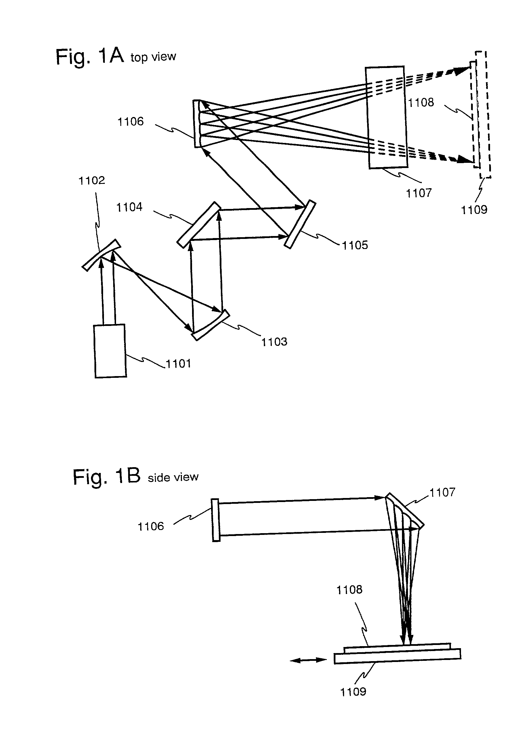
[0158] In this embodiment, an example of an optical system different from the foregoing optical system shown in FIGS. 1A and 1B will be mentioned.

[0159] FIGS. 4A and 4B show the example of the optical system in this embodiment. Excepting a reflector 1401, the construction of the optical system shown in FIGS. 4A and 4B is quite the same as that of the optical system shown in FIGS. 1A and 1B (including the reflector 1106). Therefore, regarding those parts of the optical system shown in FIGS. 4A and 4B as which the corresponding parts of the optical system shown in FIGS. 1A and 1B can be utilized as they are, the same numerals as in FIGS. 1A and 1B shall be assigned also in FIGS. 4A and 4B.

[0160] Referring to FIGS. 4A and 4B, until a laser beam reaches the reflector 1401, it passes along quite the same optical path as in the optical system shown in FIGS. 1A and 1B. The reflector 1401 is made up of a plurality of cylindrical parabolic mirrors likewise to the reflect...

embodiment 2

[0165] [Embodiment 2]

[0166] In this embodiment, an example of another optical system different from Embodiment 1 will be mentioned.

[0167] FIGS. 5A and 5B show the example of the optical system in this embodiment. Excepting a reflector 1501, the construction of the optical system shown in FIGS. 5A and 5B is quite the same as that of the optical system shown in FIGS. 1A and 1B (including the reflector 1106). Therefore, regarding those parts of the optical system shown in FIGS. 5A and 5B as which the corresponding parts of the optical system shown in FIGS. 1A and 1B can be utilized as they are, the same numerals as in FIGS. 1A and 1B shall be assigned also in FIGS. 5A and 5B.

[0168] Referring to FIGS. 5A and SB, until a laser beam reaches the reflector 1501, it passes along quite the same optical path as in the optical system shown in FIGS. 1A and 1B. The reflector 1501 is made up of a plurality of cylindrical parabolic mirrors likewise to the reflector 1106. Whereas the reflector 1106 ...

embodiment 3

[0171] [Embodiment 3]

[0172] In this embodiment, an example of another optical system different from Embodiments 1 and 2 will be mentioned.

[0173] FIGS. 6A and 6B show the example of the optical system in this embodiment. Excepting a reflector 1601, the construction of the optical system shown in FIGS. 6A and 6B is quite the same as that of the optical system shown in FIGS. 1A and 1B (including the reflector 1107). Therefore, regarding those parts of the optical system shown in FIGS. 6A and 6B as which the corresponding parts of the optical system shown in FIGS. 1A and 1B can be utilized as they are, the same numerals as in FIGS. 1A and 1B shall be assigned also in FIGS. 6A and 6B.

[0174] Referring to FIGS. 6A and 6B, until laser beams reach the reflector 1601, they pass along quite the same optical paths as in the optical system shown in FIGS. 1A and 1B. Unlike the reflector 1106, the reflector 1601 is made up of a plurality of plane mirrors. Reflected lights from the individual plane...


PUM

PropertyMeasurementUnit
lengthaaaaaaaaaa
lengthaaaaaaaaaa
thicknessaaaaaaaaaa

Abstract

An optical system (in FIGS. 1A and 1B) wherein a rectilinear laser beam of homogeneous energy distribution is defined for annealing a non-single crystalline semiconductor film (a surface to-be-irradiated 1108), is constructed of reflectors (1106, 1107 etc.) easily and inexpensively without including lenses of transmission type. The rectilinear laser beam can be defined having a length of at least 600 (mm) which corresponds to the shorter latus of a large-sized substrate for mass production.

Description

[0001] 1. Field of the Invention[0002] The present invention relates to an apparatus which homogenizes the energy distribution of a laser beam in a certain specified area. It relates also to a method for the homogenization. In addition, the present invention relates to a semiconductor device which has a circuit including a thin film transistor fabricated by the use of means for the homogenization. By way of example, it relates to the constructions of an electro-optical device which is typified by a liquid crystal display device, and an electric equipment in which such an electro-optical device is installed as a component. Incidentally, here in this specification, the expression "semiconductor device" shall signify general devices which can function by utilizing semiconductor properties, and it shall cover the electro-optical device and electric equipment mentioned above.[0003] 2. Description of the Related Art[0004] In recent years, researches have been extensively made on technique...

Claims


Application Information

Patent Timeline
Patent Type & Authority Applications(United States)
IPC IPC(8): B23K26/067B23K26/073G02B17/06H01L21/77H01L21/84
CPCB23K26/0608B23K26/067B23K26/0738G02B17/0621G02B27/0927G02B27/0983H01L21/2026H01L29/42384H01L29/458H01L29/78645H01L27/1285H01L21/02686H01L21/02683H01L21/02691H01L21/02488H01L21/02592H01L21/02422H01L21/02532H01L21/02678H01L21/02675
Inventor TANAKA, KOICHIRO
Owner SEMICON ENERGY LAB CO LTD
Why Eureka
Try Eureka