
Method of fabricating electroluminescent device using coordination metal compounds adducted with electron donor ligands as precursors

a technology of electron donor ligands and metal compounds, which is applied in the field of fabricating electroluminescent devices using coordination metal compounds adducted with electron donor ligands as precursors, can solve the problems of not having a proper chemical state, not being suitable for thin film fabrication, and difficult to form thin films with good uniformity and reproducibility

Inactive Publication Date: 2001-11-29
ELECTRONICS & TELECOMM RES INST
View PDF0 Cites 10 Cited by
  • Summary
  • Abstract
  • Description
  • Claims
  • Application Information

AI Technical Summary

Problems solved by technology

A blue-emitting phosphor material with appropriate luminance and color purity has not been developed yet, which is one of the biggest problems in the development of full color El display devices with high luminance.
Alkaline-earth thiogallates thin films that are drawing much attention as a host material of blue-emitting phosphor material do not have a proper chemical state when they are grown by the ALD method.
CaS or SrS can be used as a host material of the blue-emitting phosphor layer but are not suitable for fabrication of thin films with excellent reproducibility in large area.
The thd-compounds are easily degraded in the humid air so that it is difficult to form thin films with good uniformity and reproducibility.
When halide metal compounds are used as precursors, halogen ions are remained in an EL device as impurities thus deteriorating its function.
Doping process of metal atoms into the host material also have the same difficulty as the growth of host materials since coordination metal compounds such as thd-compounds are used.
However, the use of Pb(thd).sub.2 exhibits poor results in doping uniformity, chromaticity and luminance.

Method used


Image

  • Method of fabricating electroluminescent device using coordination metal compounds adducted with electron donor ligands as precursors
  • Method of fabricating electroluminescent device using coordination metal compounds adducted with electron donor ligands as precursors
  • Method of fabricating electroluminescent device using coordination metal compounds adducted with electron donor ligands as precursors

Examples


Embodiment Construction

[0027] Reference will now be made in detail to the preferred embodiments of the present invention, examples of which are illustrated in the accompanying drawings.

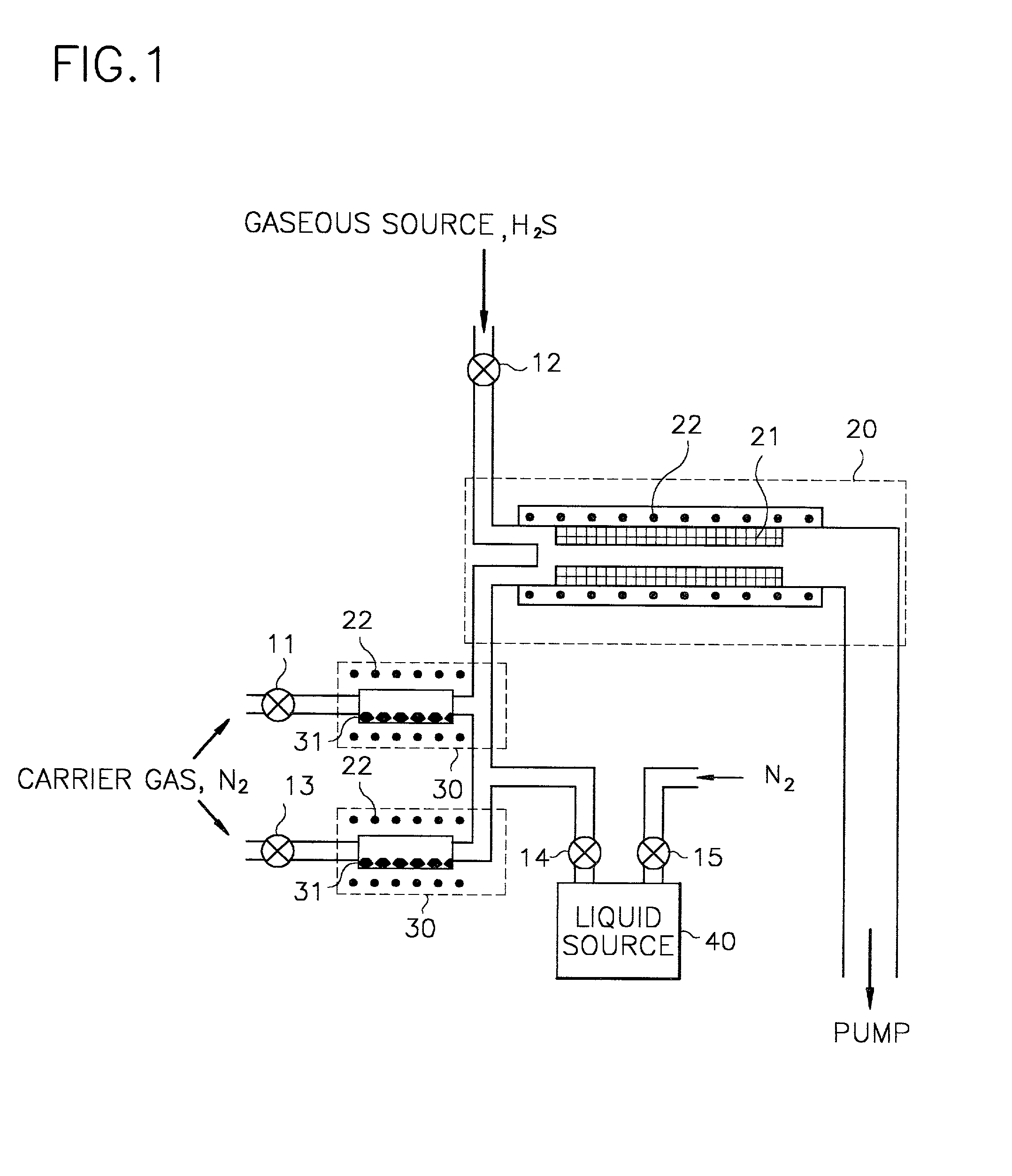
[0028] The present invention encompasses a method of fabricating thin films based on of IIA-group, IIIA-group, IVA-group, transition, or inner-transition metal sulfides or selenides by ALD or CVD method by using coordination metal compounds adducted with neutral ligands as precursors at operating pressure of 1.times.10.sup.-7 to 10 torr. The present invention also provides a method of depositing a phosphor layers of EL device with luminance by ALD or CVD method by using precursors adducted with neutral ligands selected from an amine group (NR.sub.3, R=hydrogen, methyl, ethyl, or propyl), a diamine group (ethylenediamine, 1,3-diaminopropane, and 1,2-diaminopropane), and a triamine group [N-(2-aminoethyl)-1,3-propanediamine, and diethylenetriamine]) at operating pressure of 1.times.10.sup.-7 to 10 torr.

[0029] FIG. 1 is a sche...


PUM

PropertyMeasurementUnit
Pressureaaaaaaaaaa

Abstract

A method of fabricating polycrystalline thin films based on IIA-group, IIIA-group, IVA-group, transition, or inner-transition metal sulfides or selenides by surface reaction and vapor phase reaction by using coordination metal compounds, adducted with neutral ligands and H2Z (Z=S, Se) as precursors. The present invention also discloses a method of fabricating metal oxide polycrystalline thin films based on IIA-group, IIIA-group, IVA-group, transition, or inner-transition metal oxides by surface reaction and vapor phase reaction by using coordination metal compounds, adducted with neutral ligands as one of precursors. Main object of the present invention is to provide a method of fabricating high quality EL device using the above technique.

Description

[0001] 1. Field of the Invention[0002] The present invention relates to a process of depositing metal compound thin films by an atomic layer deposition (ALD) method or chemical vapor deposition (CVD) using the coordination metal compounds adducted with electron donor ligands as precursors. The use of adducted metal compounds solves the problems caused by the use of conventional coordination metal compounds and improves the reaction stability. More particularly, it relates to deposition of metal compounds using a coordination compound adducted with neutral ligands as a precursor and a method of fabricating an electroluminescent (EL) device using the same.[0003] 2. Discussion of Related Art[0004] When metal compound films are grown by CVD or ALD method using the coordination compounds, MX.sub.n, with ligands such as 2,2',6,6'-tetramethyl-3,5-heptandione (thd), diethyldithiocarbamate (dedtc), MX.sub.n precursors are sensitive to the ambient air to be easily degraded and are affected by...

Claims


Application Information

Patent Timeline
IPC IPC(8): C23C16/30H05B33/10H05B33/14
CPCC23C16/305H05B33/10
Inventor KIM, YONG SHINYUN, SUN JINPARK, SANG HEE
Owner ELECTRONICS & TELECOMM RES INST
Learn More