

Positive chemically amplified resist and method for forming its pattern
a technology of chemical amplification and resist, which is applied in the direction of photomechanical equipment, instruments, photosensitive materials, etc., can solve the problems of resist pattern likely to be deteriorated, the laser unit itself is expensive, and the conventional resin cannot be adapted to photolithography, so as to prevent the pattern from deterioration and high adhesiveness to the substrate
- Summary
- Abstract
- Description
- Claims
- Application Information
AI Technical Summary
Benefits of technology
Problems solved by technology
Method used
Image


Examples
examples
[0060] Explanations will now be made to the resist employed in the embodiment of the present invention in comparison with some examples. Those examples will be explained for descriptive purposes only, and the present invention is not limited to those.
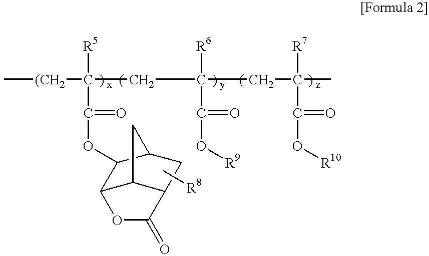
[0061] A resin for resist is compounded from the following components. In a 100 ml flask, 5-acryloyloxy-2,6-norbornanecarbolactone 6 g (0.0288 molar), t-butoxylcarbonyl tetracyclododecyl acrylate 11.975 g (0.036 molar), and carboxytetracyclododecyl methacrylate 2.193 g (0.0072 molar) are all dissolved into dry tetrahydrofuran (100 ml). In this flask, azobisisobutyronitrile 473 mg (4 molar %) is further added and reacted with the above-described components for four hours at a temperature in a range from 60.degree. C. to 65.degree. C. under argon atmosphere. After that, the solution is cooled down, and the cooled solution drips down to a solution (1,000 ml) including ligroin and toluene mixed with each other in a ratio of 4 to 1, and depo...
PUM
| Property | Measurement | Unit |
|---|---|---|
| Percent by mass | aaaaa | aaaaa |
| Wavelength | aaaaa | aaaaa |
| Wavelength | aaaaa | aaaaa |
Abstract
Description
Claims
Application Information