Electromagnetic interference analysis method and apparatus

a technology of electromagnetic interference and analysis method, applied in the field of electromagnetic interference analysis method, can solve the problems of erroneous operation, difficult implementation of such measures, and interference of electromagnetic waves in television and radio receivers

Inactive Publication Date: 2002-04-18
PANASONIC CORP
View PDF5 Cites 66 Cited by
  • Summary
  • Abstract
  • Description
  • Claims
  • Application Information

AI Technical Summary

Problems solved by technology

These devices, however, produce electromagnetic interferences, which cause electromagnetic wave interferences to television and radio receivers and erroneous operations in other systems.
Although measures to deal with these problems have been taken on the product side, such as filtering and shielding, there is a growing demand for suppressing noise of the individual LSIs themselves because such measures on the products entail increased parts count and cost and implementing such measures is not easy.
In large-scale and high-speed LSIs in which all circuits operate in synchronism with a reference clock, an instantaneous current becomes very large, increasing electromagnetic interferences.
The conductive noise, on the other hand, affects other devices on a printed circuit board through direct interconnects, such as internal wiring in the LSI, lead frames and wires on the printed circuit board.
As for signals, ringing overshoots produced by signal changes may become a problem, but variations in the LSI internal power supply level are often conducted as signal waveforms, causing problems.
This sharp change increases harmonic components and therefore the EMI.
However, because the current analysis at the transistor level uses a transient analysis simulator as represented by the SPICE, the scale of the circuit to be analyzed for EMI is limited and the processing takes very long.
In the logic simulator, however, the power supply and ground are generally treated as ideal potentials with no variations, so the influences of decoupling by resistance, capacitance and inductance of the power supply and ground cannot be reflected on the power supply current calculation.
If the influences of decoupling is to be considered, it is necessary to perform a transient analysis on the network of power supply and ground including the parasitic devices such as resistance, capacitance and inductance and on the current value of each device calculated by the logic simulation, significantly increasing the time required for processing.
Furthermore, increases in the chip scale and the number of devices have enlarged the network of power supply lines and thus an increased processing time is becoming a significant obstacle in the EMI analysis.
With this means, identifying the cause either takes very long or is impossible to perform.
Another drawback is that the analysis information provided by this means is not sufficient to be directly reflected on the correction.
As described above, the conventional EMI analysis method for LSI cannot be considered satisfactory in terms of coping with both two conditions--considering the decoupling by resistance, capacitance and inductance of the power supply and ground and increasing the processing speed--and also in terms of quickly reflecting the EMI analysis result on the design.
Although the conventional method using the transistor level current analysis technique can be expected to provide a certain level of analysis precision, as described above, because the transistor level current analysis uses a transient analysis simulator as represented by the SPICE, the size of a circuit to be analyzed is limited and the processing takes very long.
Gate level current analysis techniques have already been proposed, but they have the following problems.
Another problem is that performing the transient analysis on the power supply and ground network including parasitic devices in order to reflect the decoupling effect increases the analysis time.
A further drawback of the conventional gate level current analysis techniques is that if the EMI analysis is done, the cause of EMI cannot be identified leaving unanswered the question of which circuit should be modified for the improvement of EMI.

Method used


Image

  • Electromagnetic interference analysis method and apparatus
  • Electromagnetic interference analysis method and apparatus
  • Electromagnetic interference analysis method and apparatus

Examples


first embodiment

[0308] (First Embodiment)

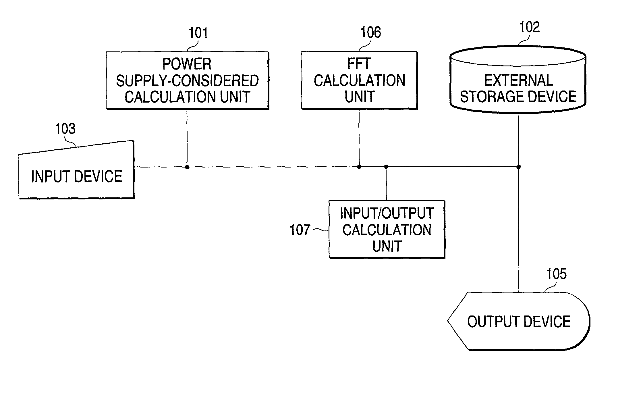
[0309] In the conventional EMI analysis of LSI, the current change that was analyzed by the power supply current transient analysis tool on transistor level is FFT-analyzed. However, because the analysis width of FFT is uniform, a problem arises that more memory is needed to store information and the analysis takes more time.

[0310] To cope with this problem, this embodiment is characterized by a frequency analysis technique in which a frequency analysis result prepared in advance and expected to have a peak is analyzed in detail and other portions of the analysis result are analyzed coarsely.

[0311] FIG. 6 shows a configuration of the EMI analysis method according to one embodiment of this invention. The EMI analysis method in the figure has a detailed frequency storage means 601, a power supply current information storage means 602, an FFT analysis means 603, and an FFT result storage means 604. Of these, the detailed frequency storage means 601, the power s...

second embodiment

[0330] (Second Embodiment)

[0331] The conventional EMI analysis of LSI is performed by FFT-analyzing the current change that was obtained by using the transient analysis tool for the transistor level power supply current. The conventional method has a problem that because the current change information is stored temporarily in a buffer, a larger amount of memory is needed for storing that information and the analysis takes longer.

[0332] To solve this problem this embodiment uses a technique of performing the frequency analysis along with the current calculation.

[0333] FIG. 11 shows a configuration of a device used for the EMI analysis method according to one embodiment of this invention. This EMI analysis apparatus has a netlist storage means 1101, a test vector storage means 1102, a current FFT analysis means 1103, and an FFT result storage means 1104.

[0334] Of these means, the netlist storage means 1101, the test vector storage means 1102 and the FFT result storage means 1104 are a...

third embodiment

[0357] (Third Embodiment)

[0358] The conventional EMI analysis method for LSI is done by FFT-analyzing the current changes that were obtained at one time for the entire analysis time span by using the transistor level power supply current transient analysis tool. This method has a problem that because the current change information is stored temporarily in the buffer, a memory for storing the information is needed.

[0359] To solve this problem this embodiment adopts a technique that performs the frequency analysis along with the current calculation for each predetermined time interval.

[0360] FIG. 16 shows a configuration of a device used for the EMI analysis method according to one embodiment of this invention.

[0361] The EMI analysis apparatus shown comprises a netlist storage means 1601, a test vector storage means 1602, a current FFT analysis means 1603, an FFT result storage means 1604, and a power supply current storage means 1605.

[0362] Of these, the netlist storage means 1601, t...


PUM


Abstract

This invention is characterized to include a discrete analysis frequency width change specifying process for specifying in a particular frequency range a change in the discrete high-speed Fourier transform (FFT) analysis frequency width and a modeling process for allocating different discrete FFT analysis frequency widths to the specified frequency range and to a frequency range other than the specified frequency range and performing modeling. The EMI analysis method of this invention reflects on the gate level power supply current calculation the influence of decoupling by resistance, capacitance and inductance of the power supply and ground, thereby making it possible to evaluate the EMI of LSIs in simulation in a realistic time and to provide efficient EMI countermeasures through supporting the identifying of the EMI causing locations.

Description

[0001] 1. Field of the Invention[0002] The present invention relates to a method of analyzing electromagnetic interference (EMI) and more particularly to a method of analyzing EMI by performing a high-speed, high-precision logic simulation on a large and high-speed LSI (large-scale integrated circuit).[0003] 2.Description of the related Art[0004] LSIs have found a wide range of applications, including computers, communication devices such as cellular phones, home products, toys, and automobiles. These devices, however, produce electromagnetic interferences, which cause electromagnetic wave interferences to television and radio receivers and erroneous operations in other systems. Although measures to deal with these problems have been taken on the product side, such as filtering and shielding, there is a growing demand for suppressing noise of the individual LSIs themselves because such measures on the products entail increased parts count and cost and implementing such measures is n...

Claims


Application Information

Patent Timeline
Patent Type & Authority Applications(United States)
IPC IPC(8): G01R31/00G06F17/50G01R29/08
CPCY02T10/82G01R31/002
Inventor SHIMAZAKI, KENJIHIRANO, SHOUZOUTSUJIKAWA, HIROYUKIMIZOKAWA, TAKASHI
Owner PANASONIC CORP
Why Eureka
Try Eureka