Automatic cell placement and routing apparatus and automatic cell placement and routing method used for the apparatus

a cell placement and automatic technology, applied in the direction of instruments, cad circuit design, computer aided design, etc., can solve the problems of difficult widening of the interval crowded cell area, and inability to reduce the capacitance between the adjacent wires

Inactive Publication Date: 2002-04-18
RENESAS ELECTRONICS CORP
View PDF1 Cites 20 Cited by
  • Summary
  • Abstract
  • Description
  • Claims
  • Application Information

AI Technical Summary

Benefits of technology

[0009] In the above configuration, because the cross-talk noise improving cell embedded in the hard macro-block is inserted into a wire of the semiconductor integrated circuit, the capacitance between the wire and an adjacent wire is reduced.
[0042] Accordingly, the cross-talk noise can be reduced without increasing an area of the semiconductor integrated circuit.

Problems solved by technology

However, it is impossible to reduce a capacitance between wires adjacent to each other in a crowded cell area such as a peripheral area of a hard macro-block (for example, a mega-cell such as a read only memory (ROM) cell or a random access memory (RAM) cell and an input-output (IO) cell) in which the insertion of a buffer cell is difficult, a cell insertion inhibit area and a crowded wire area in which the widening of an interval between wires adjacent to each other is difficult.
Therefore, because the above-described method is adopted in the conventional automatic cell placement and routing apparatus, there is a problem that it is impossible to reduce the cross-talk noise in the crowded cell area, the cell insertion inhibit area and the crowded wire area.

Method used


Image

  • Automatic cell placement and routing apparatus and automatic cell placement and routing method used for the apparatus
  • Automatic cell placement and routing apparatus and automatic cell placement and routing method used for the apparatus
  • Automatic cell placement and routing apparatus and automatic cell placement and routing method used for the apparatus

Examples


first embodiment

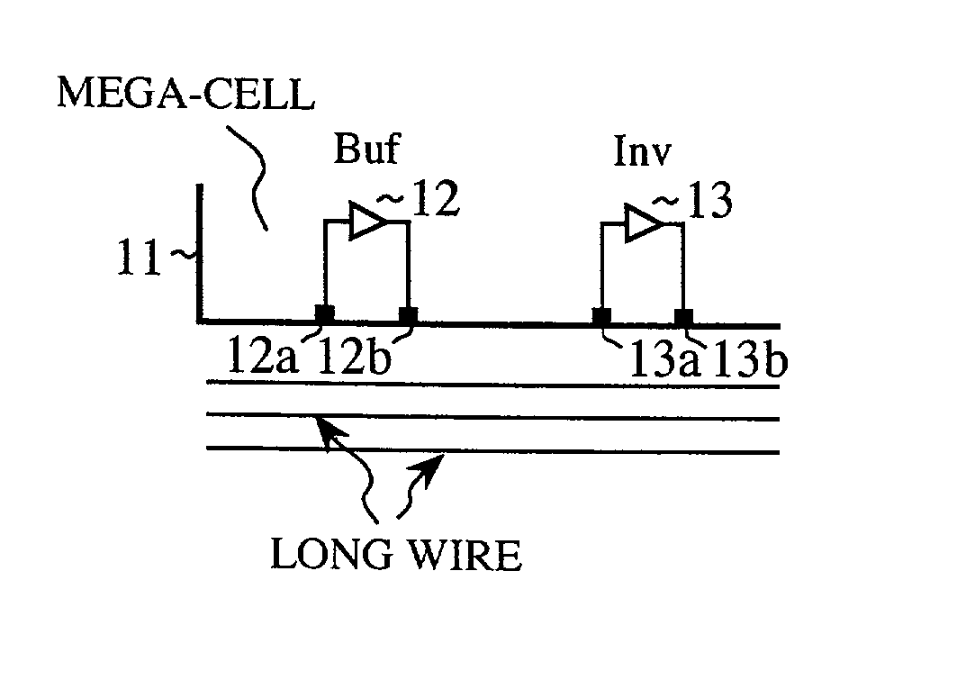
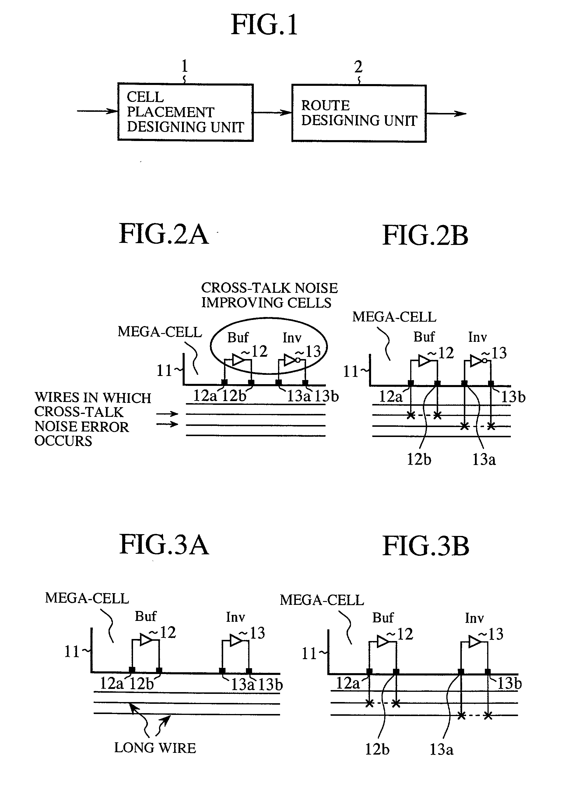
[0086] Therefore, in the first embodiment, when a layout of cells composing a semiconductor integrated circuit is designed by the cell placement designing unit 1 of the automatic cell placement and routing apparatus, as shown in FIG. 2A, the buffer cell 12 and / or the inverter cell 13 denoting the cross-talk improving cells are embedded in advance in an internal open space of each of mega-cells 11 and IO cells.

[0087] Thereafter, in the route designing unit 2 of the automatic cell placement and routing apparatus, when it is expected that a cross-talk noise is generated in a signal (or signals) transmitting through a wire (or wires) of the semiconductor integrated circuit, as shown in FIG. 2A, a mega-cell 11 (or an IO cell), which is placed in a position nearest to a generation position of the cross-talk noise, is selected from the mega-cells 11 and the IO cells. Thereafter, as shown in FIG. 2B, the buffer cell 12 and / or the inverter cell 13 embedded in the internal of the selected meg...

embodiment 2

[0089] EMBODIMENT 2

[0090] In the first embodiment, the buffer cell 12 and the inverter cell 13 embedded in the internal open space of the mega-cell 11 or the IO cell are inserted into wires in which signal error occurs because of the influence of the cross-talk noise. However, in general, a wire having a long wire length is liable to be influenced by the cross-talk noise. Therefore, in a second embodiment, as shown in FIG. 3A, one or more wires, which extend through the neighborhood of the mega-cell 11 or the IO cell, are selected from wires which respectively have a wire length equal to or longer than a prescribed value. Thereafter, as shown in FIG. 3B, the buffer cell 12 and the inverter cell 13 embedded in the internal open space of the mega-cell 11 or the IO cell are inserted into the selected wires to shorten the length of each selected wire.

[0091] Accordingly, the adverse influence of the cross-talk noise generated in the semiconductor integrated circuit can be reduced.

embodiment 3

[0092] EMBODIMENT 3

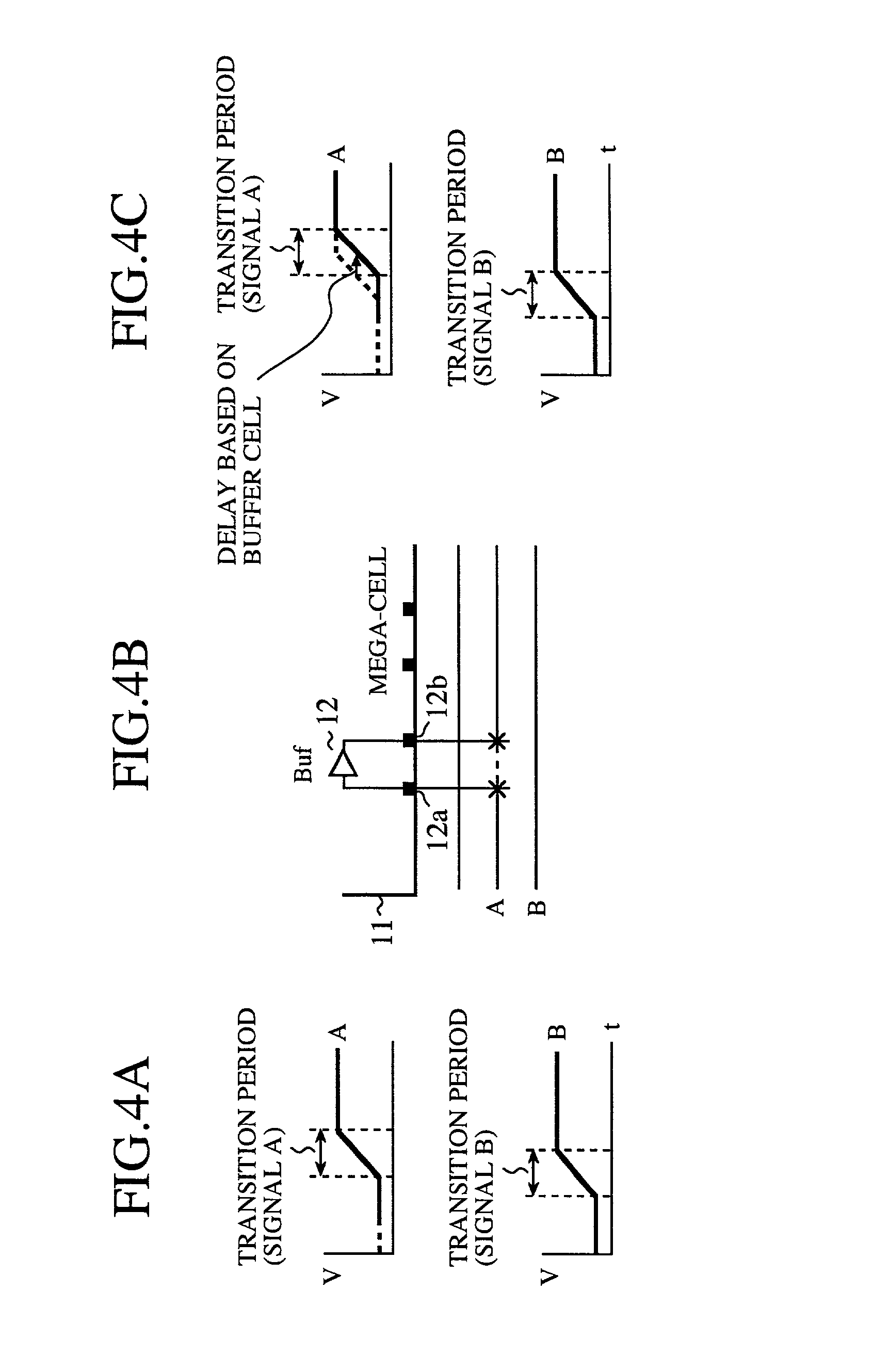
[0093] In the first embodiment, the buffer cell 12 and the inverter cell 13 embedded in the internal open space of the mega-cell 11 or the IO cell are inserted into wires in which signal error occurs because of the influence of the cross-talk noise. However, in a third embodiment, when a level transition period of a signal transmitting through a wire overlaps with that of a signal transmitting through another wire on condition that the wires are adjacent to each other, the cross-talk noise improving cell is inserted into one of the wires to make the level transition periods of the signals not overlap with each other.

[0094] In detail, in the route designing unit 2, level transition periods of signals A and B, which transmit through wires adjacent to each other, are calculated according to a dynamic or static timing analysis. In general, when level transition periods of signals transmitting through wires adjacent to each other overlap with each other, the signals ar...


PUM


Abstract

A buffer cell and an inverter cell are embedded in advance in an internal open space of each of mega-cells and IO cells composing a semiconductor integrated circuit. Thereafter, in cases where it is expected that a cross-talk noise is generated in a signal transmitting through a particular wire of the semiconductor integrated circuit, one mega-cell or one IO cell, which is placed in a position nearest to a generation position of the cross-talk noise, is selected from the mega-cells and the IO cells, and the buffer cell or the inverter cell embedded in the selected mega-cell or the selected IO cell is inserted into the particular wire. Therefore, because the capacitance between the particular wire and each wire adjacent to the particular wire is reduced, the cross-talk noise can be reduced.

Description

[0001] 1. Field of the Invention[0002] The present invention relates to an automatic cell placement and routing apparatus in which a layout of cells composing a semiconductor integrated circuit is designed not to receive an adverse influence of a cross-talk noise generated when the semiconductor integrated circuit is actually operated. Also, the present invention relates to an automatic cell placement and routing method used for the apparatus.[0003] 2. Description of Related Art[0004] When a layout of cells composing a semiconductor integrated circuit is designed, to reduce cross-talk noise generated in the semiconductor integrated circuit, a method for widening an interval between wires adjacent to each other and / or inserting a buffer cell or an inverter cell into a wire is adopted in a conventional automatic cell placement and routing apparatus. Therefore, a capacitance between wires adjacent to each other is reduced, and the cross-talk noise is reduced.[0005] This automatic cell ...

Claims


Application Information

Patent Timeline
Patent Type & Authority Applications(United States)
IPC IPC(8): G06F17/50H01L21/82H01L21/822H01L27/04
CPCG06F17/5068G06F30/39
Inventor HIRAKIMOTO, KOJISAITO, KENUMEDA, TATSUYA
Owner RENESAS ELECTRONICS CORP
Why Eureka
Try Eureka