Memory cell structure of flash memory having circumventing floating gate and method for fabricating the same
- Summary
- Abstract
- Description
- Claims
- Application Information
AI Technical Summary
Benefits of technology
Problems solved by technology
Method used
Image

Examples
Embodiment Construction
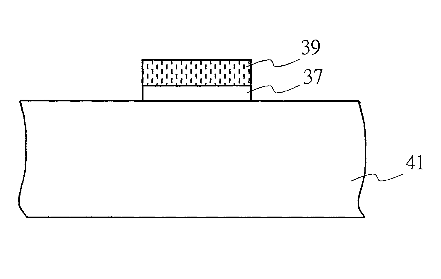
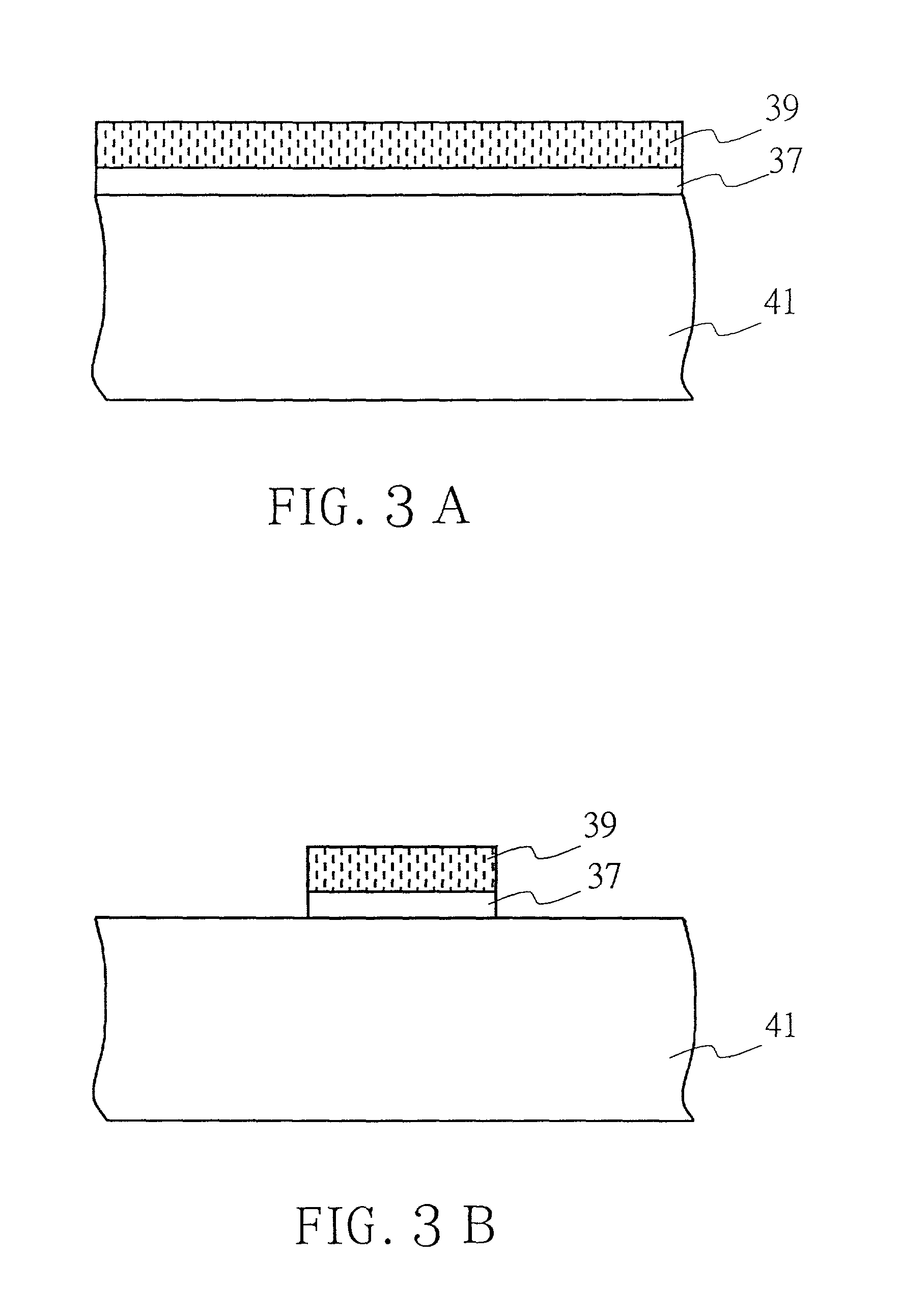
[0019] As shown in FIG. 5, the memory cell structure of a flash memory according to a preferred embodiment of the present invention comprising: a semiconductor substrate 41 having a source 42 and a drain 44 therein. An annular floating gate 45 has part region thereof covering on the surfaces of said source 42 and said drain 44, and a tunneling oxide 43 electrically insulates the source 42 and the drain 44. Said substrate 41 being exposed in the carved-out center of said floating gate 45. An interpoly dielectric 47 covering on the surface of said floating gate 45, on the center of said floating gate 45, and on the surface of said substrate 41 exposed at the periphery of said floating gate 45, and a control gate 49 covers on the surface of said interpoly dielectric 47.
[0020] Additionally, the floating gate is an annular shape formed by poly-silicon spacers, and the interpoly dielectric 47 is an oxide-nitride-oxide (ONO) structure or an oxide-nitride (ON) structure of good dielectric c...
PUM
 Abstract
Description
Claims
Application Information