

Optical disk and method for producing the same
a technology of optical disks and optical disks, applied in the field of optical disks, can solve the problem of long initialization tim
- Summary
- Abstract
- Description
- Claims
- Application Information
AI Technical Summary
Benefits of technology
Problems solved by technology
Method used
Image

Examples
embodiment 1
[0055] As described above, , an optical disk with a high recording density is obtained that can be initialized in a short period of time.
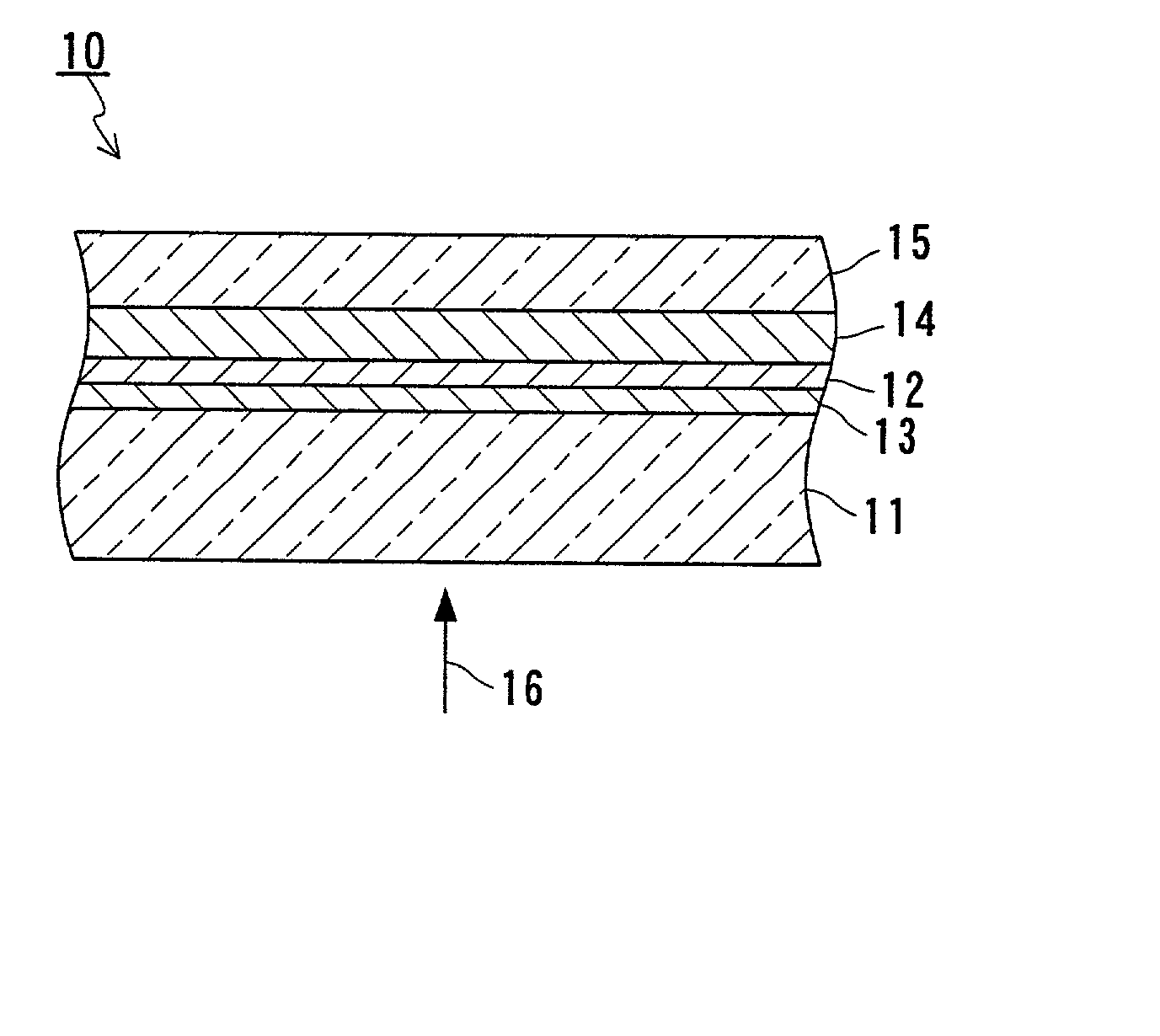
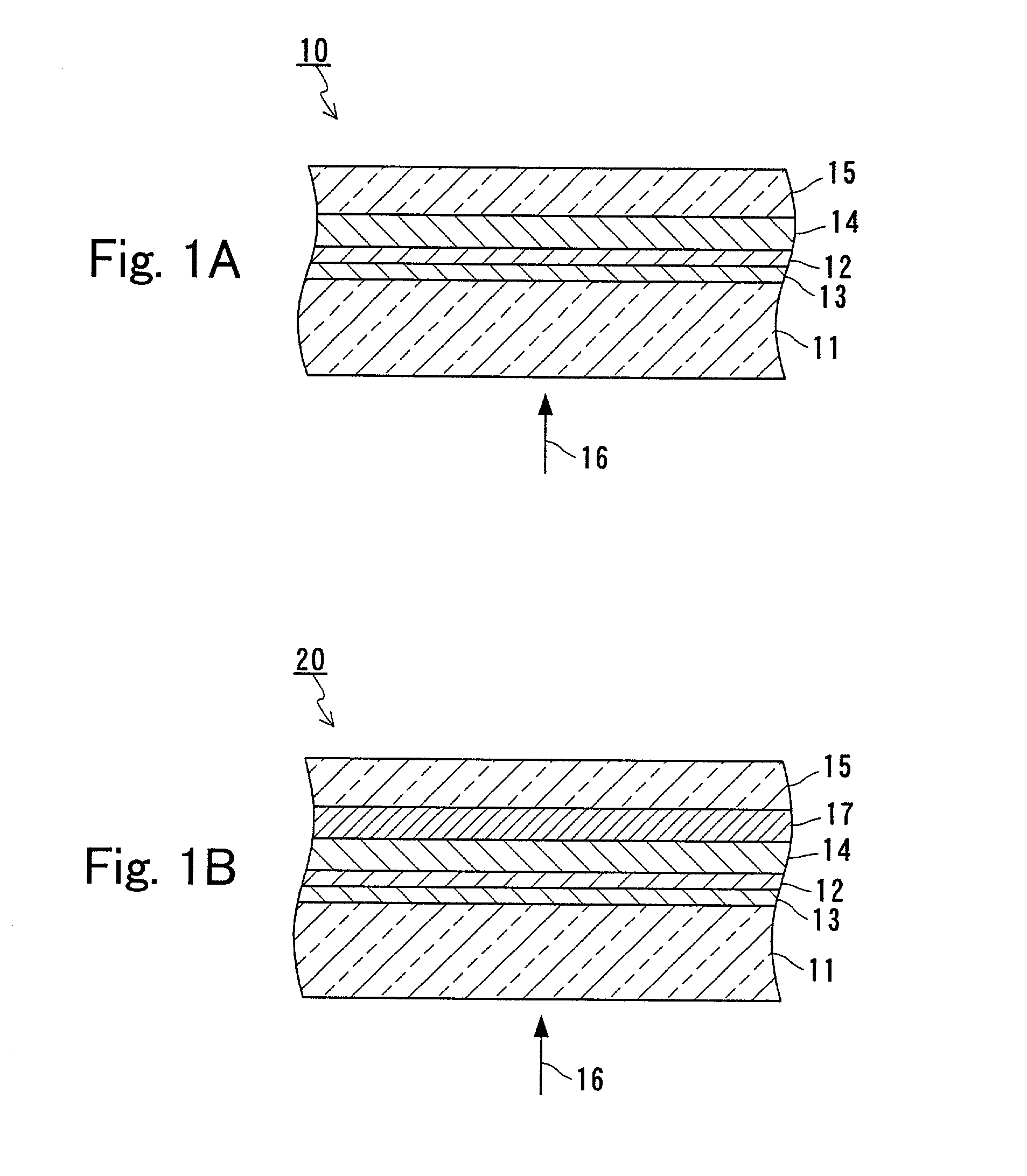
[0056] The optical disk 10 of the present invention further may include a heat conduction adjusting layer for adjusting the sensitivity of the recording layer 12 between the second dielectric layer 14 and the protective coating layer 15. FIG. 1B is a partial cross-sectional view of an optical disk 20 having a heat conduction adjusting layer 17. As the heat conduction adjusting layer 17, a metal film can be used. For example, a film made of aluminum or gold can be used. The thickness of the heat conduction adjusting layer 17 generally is about 50 nm to about 500 nm.
embodiment 2
[0057] In Embodiment 2, an example of a method for producing an optical disk according to the present invention will be described. Embodiment 2 is directed to a method for producing an optical disk that reproduces an information signal by the DWDD system, using light incident on a substrate side. In Embodiment 2, the case will be described in which the optical disk 10 of Embodiment 1 is produced. Furthermore, the same components as those described in Embodiment 1 are denoted with the same reference numerals as those therein, and a repeated description thereof will be omitted herein (this also applies to the other embodiments).
[0058] According to the production method of Embodiment 2, the first dielectric layer 13, the recording layer 12, and the second dielectric layer 14 are formed on the substrate 11 in this order (hereinafter, this process may be referred to as "Process (i)"). These layers can be formed continuously by, for example, sputtering using a magnetron sputtering apparat...
embodiment 3
[0071] Embodiment 3, another exemplary method for producing an optical disk according to the present invention will be described. The production method of Embodiment 3 is different from that of Embodiment 2 only in the initialization process (Process (ii)). Therefore, a repeated description thereof will be omitted here.
[0072] Hereinafter, the initialization method of Embodiment 3 will be described. FIG. 6 schematically shows a structure of an initialization apparatus 60 used by the production method of Embodiment 3.
[0073] Referring to FIG. 6, the initialization apparatus 60 includes a laser light source 31 for annealing, laser beam splitters 32, 62 and 65, a focus detector 33, an objective lens 34, a focus actuator 35, a laser light source 61 for tracking servo, a photodetector 63, and a tracking actuator 64.
[0074] An operation of the initialization apparatus 60 will be described with reference to FIG. 6. Laser light L2 emitted from the laser light source 61 passes through the beam ...
PUM
| Property | Measurement | Unit |
|---|---|---|
| Thickness | aaaaa | aaaaa |
| Thickness | aaaaa | aaaaa |
| Thickness | aaaaa | aaaaa |
Abstract
Description
Claims
Application Information