

Clock control circuit and method
a control circuit and clock technology, applied in the direction of generating/distributing signals, pulse techniques, instruments, etc., can solve the problem of difficult to generate correctly a signal of a desired phas
- Summary
- Abstract
- Description
- Claims
- Application Information
AI Technical Summary
Benefits of technology
Problems solved by technology
Method used
Image

Examples
first embodiment
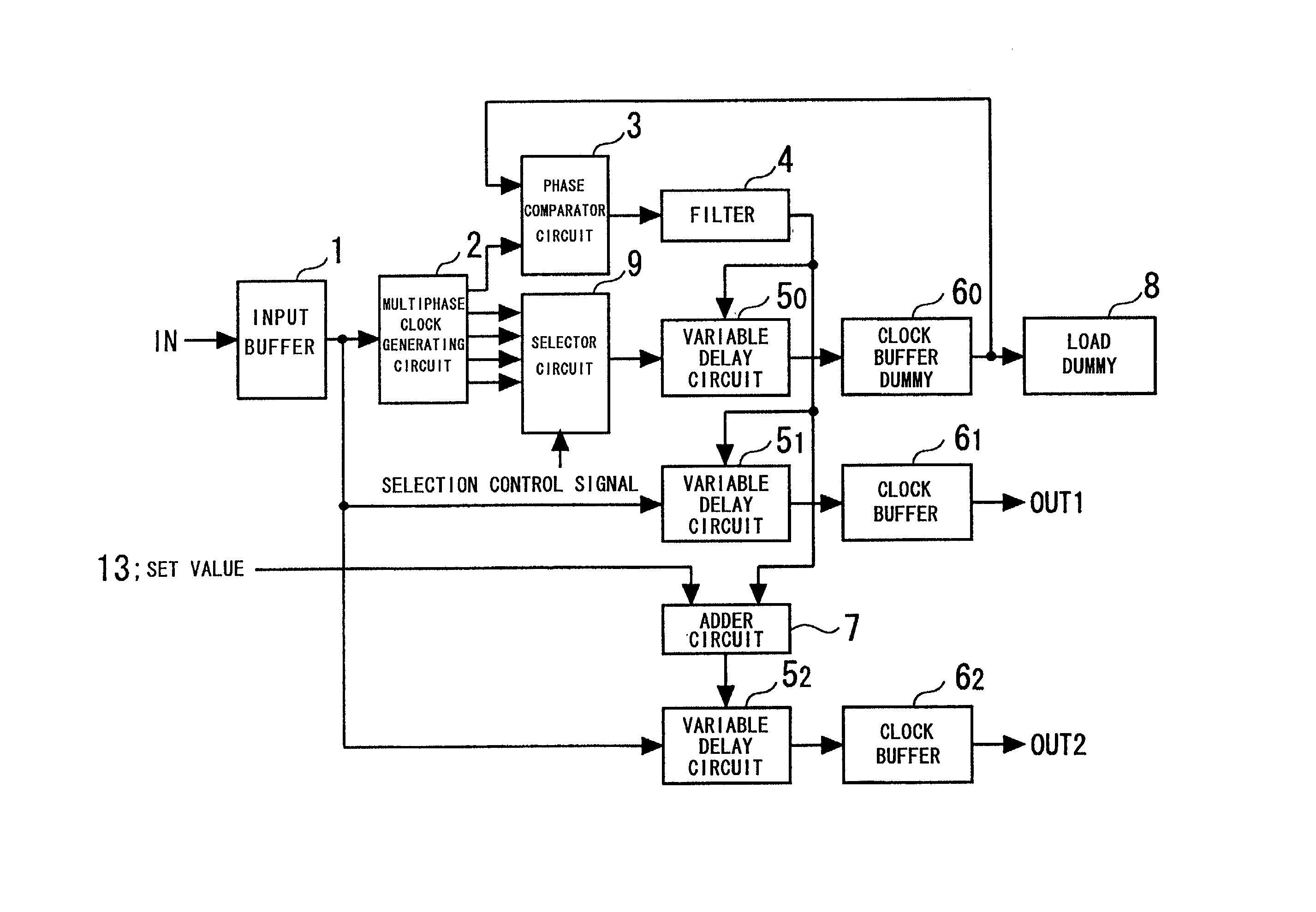
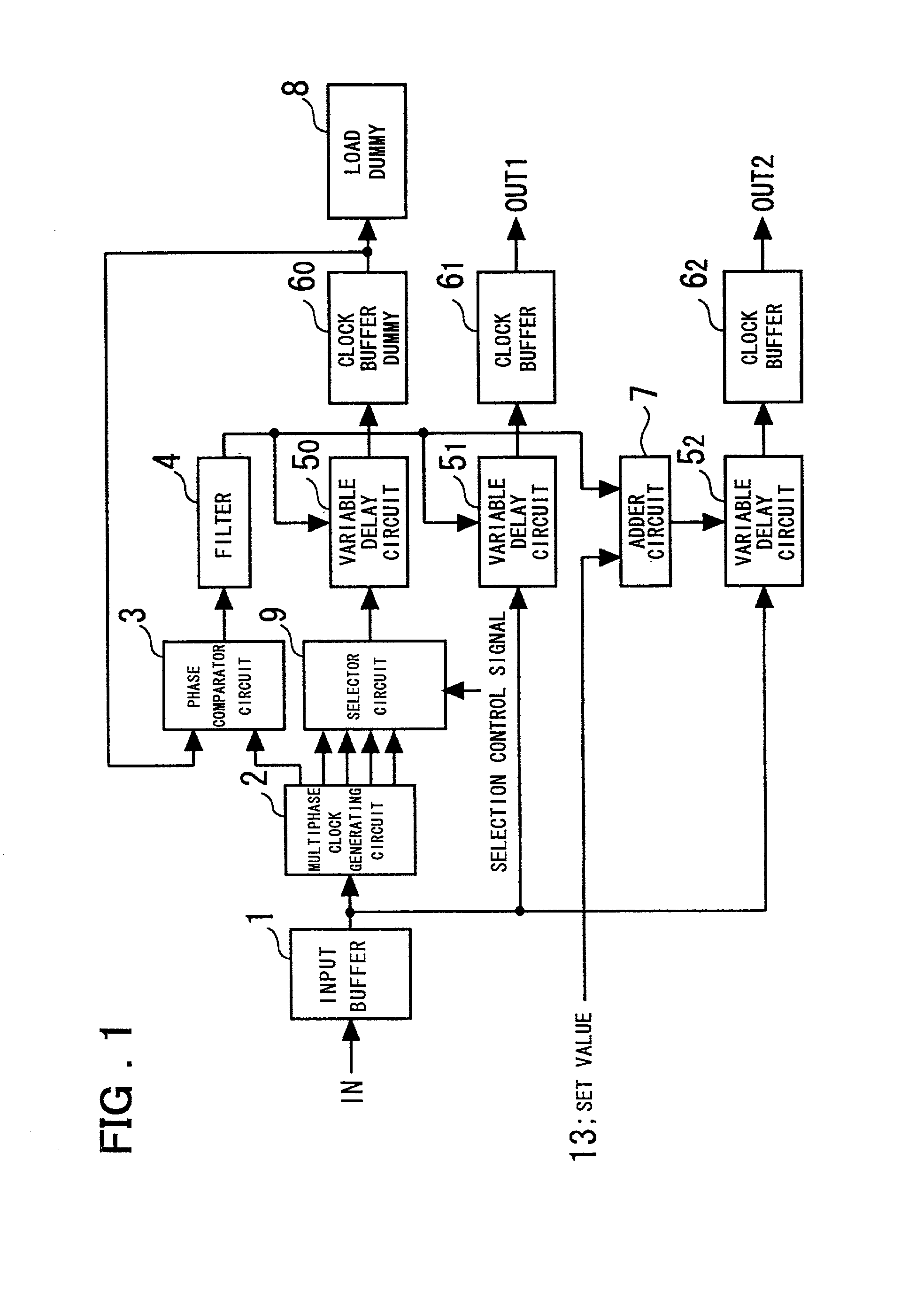
[0068] The operation of the invention shown in FIG. 1 will now be described.
[0069] The selector circuit 9 selects a clock (a clock having an ith phase), which has a prescribed phase relationship with respect to the clock supplied to the phase comparator circuit 3, from among the multiphase clocks output from the multiphase clock generating circuit 2. The phase comparator circuit 3 is controlled in such a manner that the delay time of the variable delay circuit 50 and clock buffer dummy 60 will become equal to this phase difference, the output OUT1 delivers a first clock signal having a desired phase difference with respect to the input clock, and the output OUT2 delivers a second clock signal having a desired phase difference with respect to the first clock signal output from the output OUT1. The selection made by the selector circuit 9 may be in response to a selection control signal from a CPU (not shown) or a selection control signal that is applied externally. For example, if th...
second embodiment
[0092] As for the generation of the phase difference, several arrangements are applicable in addition to the above-described arrangement of the multiphase clock generating circuit and selector circuit. the invention having an interpolator-based phase-difference generating circuit will be described next.
[0093] FIG. 8 is a block diagram illustrating the structure of a second embodiment of the present invention.
[0094] As shown in FIG. 8, a clock control circuit in accordance with the second embodiment of the invention comprises: a phase-difference generating circuit 10, to which the output signal of the input buffer 1 is provided, for outputting first and second signals a, b obtained by delaying the output signal of input buffer 1 by a predetermined phase difference on the basis of a phase decision information 14 received; the variable delay circuit 5.sub.0 for delaying the second output b of the phase-difference generating circuit 10; the clock buffer dummy 6.sub.0 for driving the out...
third embodiment
[0115] the present invention will now be described.
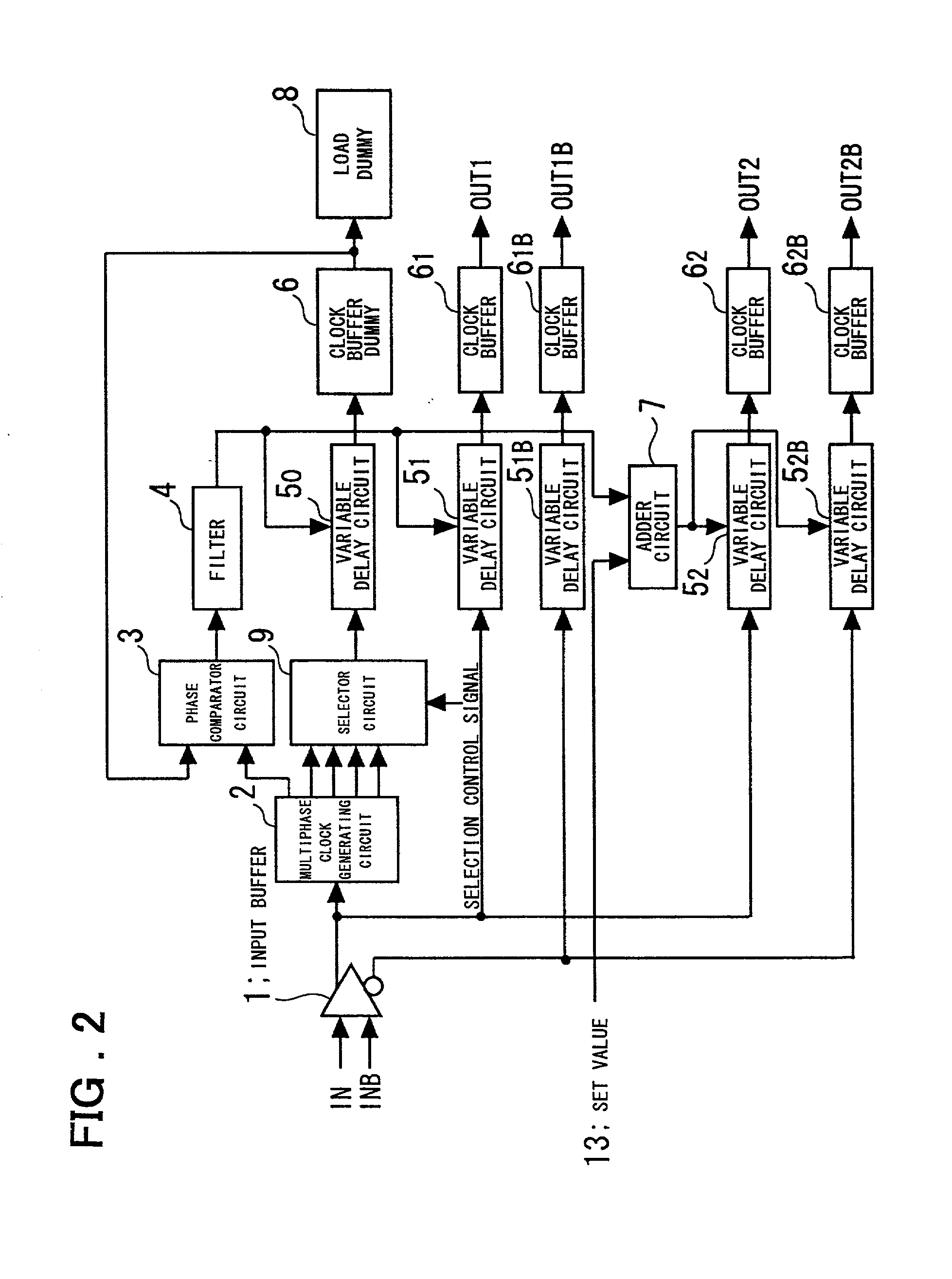
[0116] FIG. 12 is a diagram showing the structure of the third embodiment of the invention. As shown in FIG. 12, the third embodiment of the invention comprises: a phase-difference generating circuit (10A), to which an output signal of the input buffer 1 and an output signal of the clock buffer 6.sub.1 are input, for outputting two signals having a desired phase difference between them from the output (in-phase output) of the input buffer 1 and the output of the clock buffer 6.sub.1 on the basis of the phase decision information 13; the phase comparator circuit 3 for comparing the phases of the two outputs of the phase-difference generating circuit 10A; a filter 4 for smoothing the output of the phase comparator circuit 3; variable delay circuits 5.sub.1, 5.sub.1B for delaying in-phase and reverse-phase complementary outputs, respectively, of the input buffer 1; and clock buffers 6.sub.1, 6.sub.1B for driving the outputs of the vari...
PUM
 Abstract
Description
Claims
Application Information