Surge absorber without chips

a technology of shock absorber and absorber, which is applied in the field of shock absorber without chips, can solve the problems of damage to semiconductors or devices themselves, severe limitations in their use, and complex structur

Inactive Publication Date: 2002-06-20
YANG BING LIN
View PDF16 Cites 15 Cited by
  • Summary
  • Abstract
  • Description
  • Claims
  • Application Information

AI Technical Summary

Benefits of technology

[0019] According to the present invention wherein the discharge electrodes are formed by broadening the tips of the lead terminals, discharge electrodes having a variety of sizes can be obtained from lead terminals having identical diameters by changing the degree of the broadening. Moreover, as the discharge electrodes of the present invention do not need to be fixed on the housing, discharge electrodes of different diameters can be placed inside housings having common sizes. By using lead terminals and housings both having identical diameters, and by selecting a variety of sizes of broadened diameters for lead terminal tips, surge absorbers corresponding to different levels of surge voltages can be provided easily.
[0031] Moreover, the surge absorber without chips according to the present invention can also be used in devices to be connected to telephone lines, such as a telephone set, a radio, a facsimile, a modem, and a program-controlled telephone switching device, devices to be connected to antennas or signal wires, such as an amplifier, a tape recorder, a vehicle radio, a radio transceiver, and a sensor signal wire, devices requiring prevention of static electricity, such as a display and a monitor, domestic appliances, and computer controlled electronic devices. The surge absorber without chips of the present invention also functions as an over-voltage prevention device. In other words, the surge absorber is an electronic element effective for counteracting hazardous influences of electric noise.

Problems solved by technology

Stray waves, noise, and electrostatic disturbances which may cause surges are deeply-rooted obstacles to the most up-to-date electronic devices.
In particular, high voltage pulse waves cause erroneous operations of semiconductor elements in electronic devices, and sometimes even damage the semiconductors or the devices themselves.
However, as it is difficult to freely select a switching voltage in surge absorbers of this type, uses thereof are severely limited.
The structure is therefore complex and requires many manufacturing processes, making it difficult to reduce production costs.
In this situation, the problem exists wherein the number of surge absorbers used leads directly to the increase in cost of the overall equipment.
These surge absorbers are therefore unable to cope with a high switching voltage of, for example, 10,000 volts, and cannot completely absorb a surge of large energy at the time of surge absorption.
This causes the problem that, due to the residual voltage, a follow-current (a current, caused by a residual voltage, that flows into the electronic equipment to be protected) is generated in the circuitry.
Further, in conventional devices, it is a problem that the switching voltage varies depending on the specification of the tube core.
Using this structure, it is therefore practically impossible to obtain a surge absorber without chips that is applicable to a wide range of discharge voltages and maximum surge current.
Under these circumstances, heat welding can not be used, and fusing must be performed at the contacting surfaces of the insulating tube and the electrodes.
During the fusing process, the air chamber becomes severely contaminated by flux or the like, resulting in extreme deterioration of the discharge characteristics.
Moreover, as gas resistance in the air chamber is notably low at the time of insulation discharge, the operational resistance can be extremely low when the dielectric breakdown of the gas is caused by a surge voltage.

Method used


Image

  • Surge absorber without chips
  • Surge absorber without chips
  • Surge absorber without chips

Examples


Embodiment Construction

[0053] Preferred embodiments of the present invention will now be described referring to the accompanying drawings.

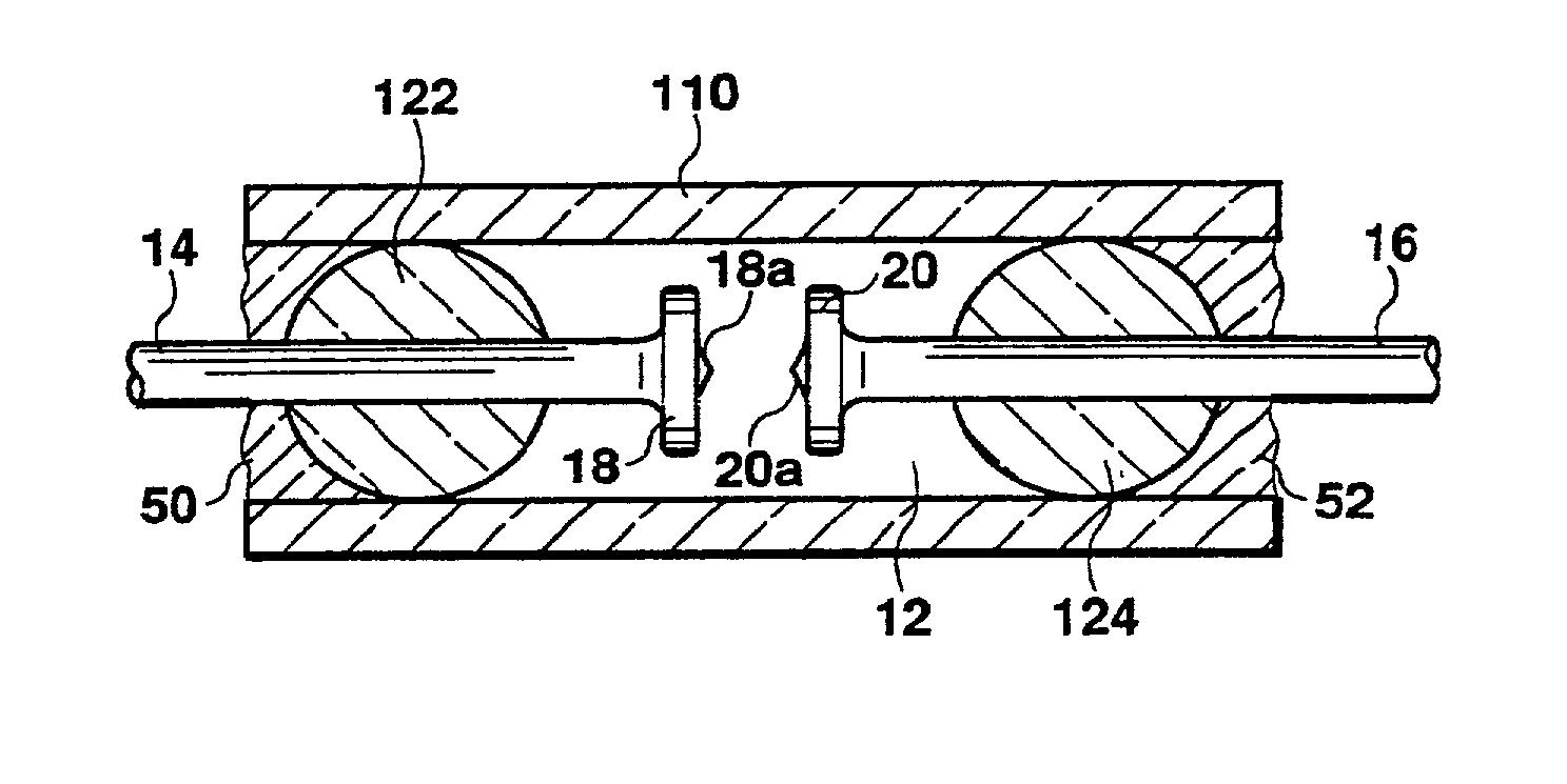
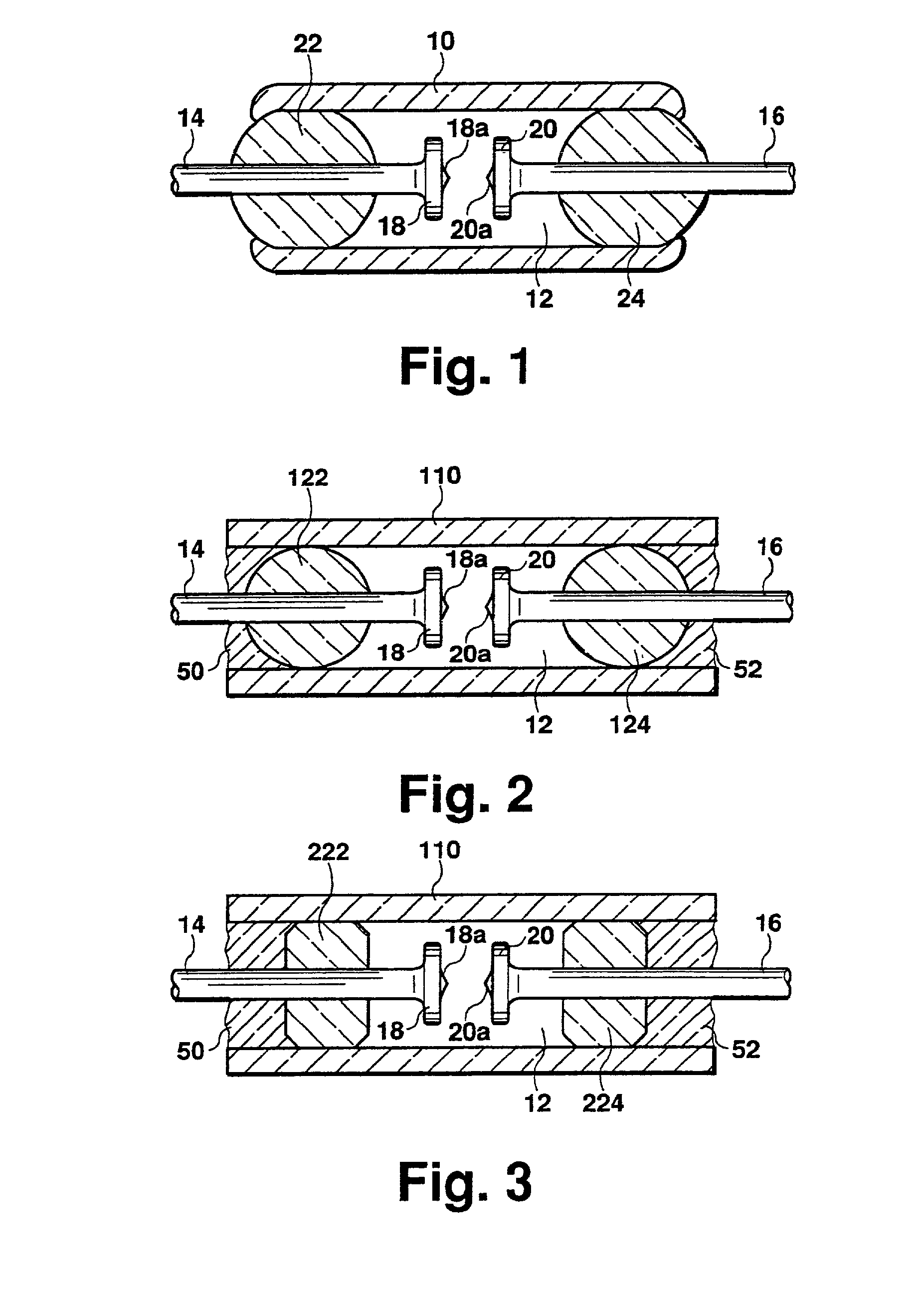
[0054] FIG. 1 shows a preferred embodiment of a surge absorber without chips of the present invention. A housing 10 comprises a glass or plastic cylinder, and an air chamber 12 is provided inside the housing. Lead terminals 14,16 are inserted from openings on both ends of the housing 10. In the air chamber 12, discharge electrodes 18,20 formed by broadening the diameter of the tips of the lead terminals 14,16 are arranged facing one another at a predetermined distance.

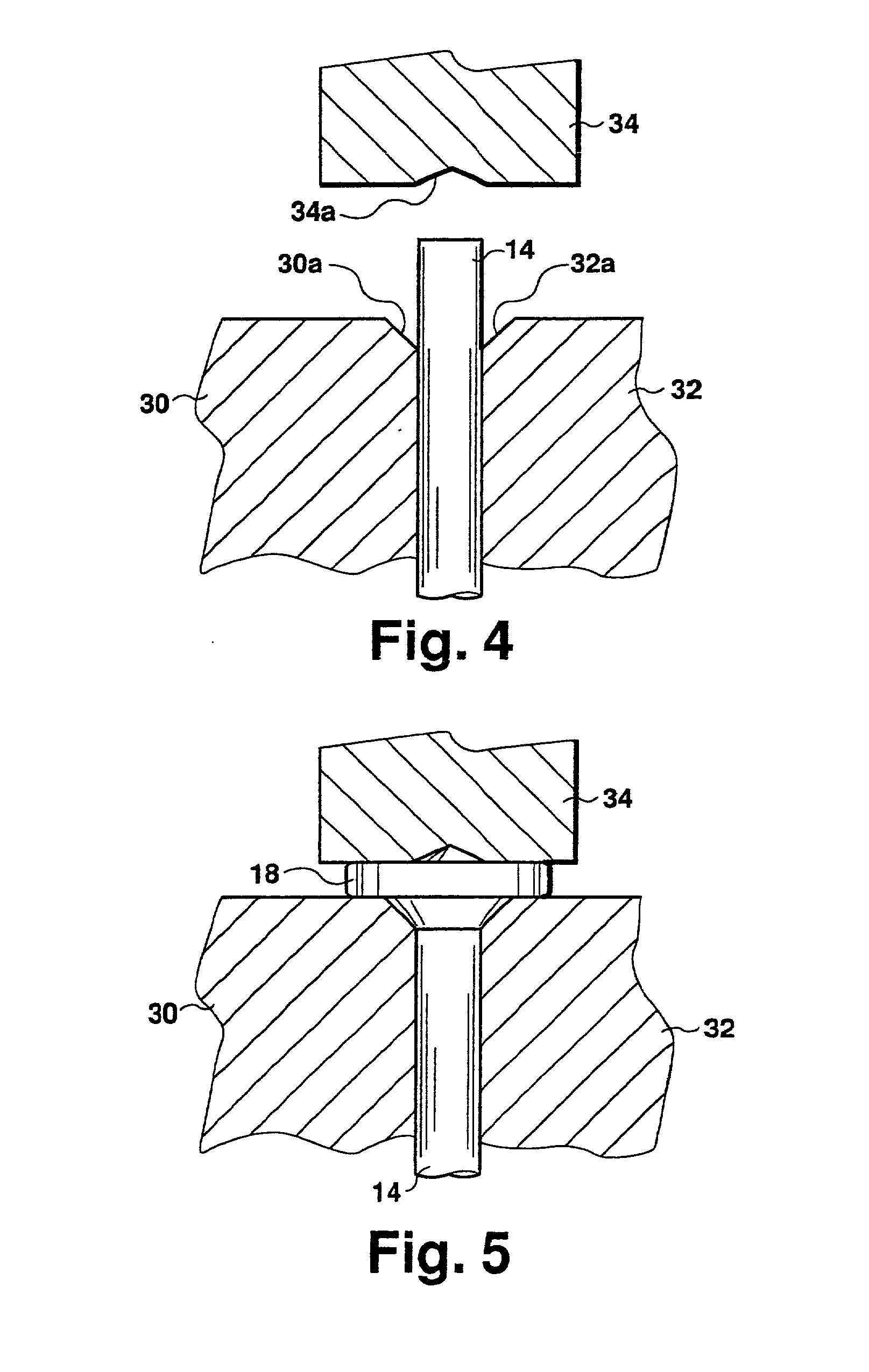
[0055] The feature of the present invention is that the discharge electrodes 18,20 are formed by broadening the diameter of respective tips of the lead terminals 14,16. The broadening process is described later in detail.

[0056] Protruding portions 18a,20a are formed in the center of each of the discharge electrodes 18,20. With this arrangement, when a surge voltage is applied to the lead terminals 14,16, a...


PUM


Abstract

There is provided a surge absorber without chips that has a simple structure, has a broad range of surge switching voltage, and can perform stable surge absorption. Discharge electrodes 18,20 are formed on tips of lead terminals 14,16 by pressing. Sealing spacers 22,24 are welded on the lead terminals 14,16. These spacers 22,24 are inserted inside a housing 10 and fixed on the housing 10 by welding. Discharge electrodes 18,20 having different diameters can be arbitrarily formed on lead terminals having identical diameters.

Description

[0001] 1. Field of the Invention[0002] The present invention relates to an electronic element, and in particular, to a surge absorber without chips.[0003] 2. Description of the Background Art[0004] Stray waves, noise, and electrostatic disturbances which may cause surges are deeply-rooted obstacles to the most up-to-date electronic devices. In particular, high voltage pulse waves cause erroneous operations of semiconductor elements in electronic devices, and sometimes even damage the semiconductors or the devices themselves. Such problems can, however, be solved by the use of surge absorbers.[0005] A conventional surge absorber comprises a discharge chip or discharge core having an insulating microgap, and this discharge chip is sealed in a glass housing. For example, in a microgap surge absorber manufactured by Mitsubishi Materials K.K., a thin conductive film is developed on a ceramic core, and cap-shaped metal electrodes are fixed on both ends of the core. Subsequently, the surfa...

Claims


Application Information

Patent Timeline
Patent Type & Authority Applications(United States)
IPC IPC(8): H01T1/22H01T4/10H01T4/04H01T4/12H01T21/00
CPCH01T4/12H01L24/01H01T21/00H01L2924/12042H01L2924/12041H01L2924/00H01L23/60
Inventor YANG, BING LIN
Owner YANG BING LIN
Why Eureka
Try Eureka