Semiconductor device and method of fabricating the same

a semiconductor and device technology, applied in the field of high-integrated semiconductor devices, can solve the problems of dram cells degrading in operation margins, unable to achieve the required capacitance, and unable to meet the requirements of capacitance,

Inactive Publication Date: 2002-06-20
KK TOSHIBA
View PDF1 Cites 206 Cited by
  • Summary
  • Abstract
  • Description
  • Claims
  • Application Information

AI Technical Summary

Problems solved by technology

With regard to cell capacitors, one major problem to be solved is how the required amount of capacitance is achieved while at the same time reducing or minimizing onchip cell areas.
However, an increase in substrate impurity concentration would result in an increase in junction current leakage between a substrate and storage nodes, which in turn leads to decreases in data-retaining / holding abilities of memory cells, as suggested for example by T. Hamamoto et al., "Well concentration: A novel scaling limitation factor derived from DRAM retention time and its modeling," International Electron Devices Meeting (IEDM) Technical Digest at page 915 (1995).
This gives rise to a risk that DRAM cells degrade in operation margins.
Unfortunately, the advantage of the above-stated DRAM cell structure does not come without accompanying a penalty--the vertical transistor Q can readily vary in channel length through effectuation of etch-back processes.
The channel length irregularity can cause a problem as to undesired variation or deviation of transistor characteristics.

Method used


Image

  • Semiconductor device and method of fabricating the same
  • Semiconductor device and method of fabricating the same
  • Semiconductor device and method of fabricating the same

Examples


embodiment 1

[Embodiment 1]

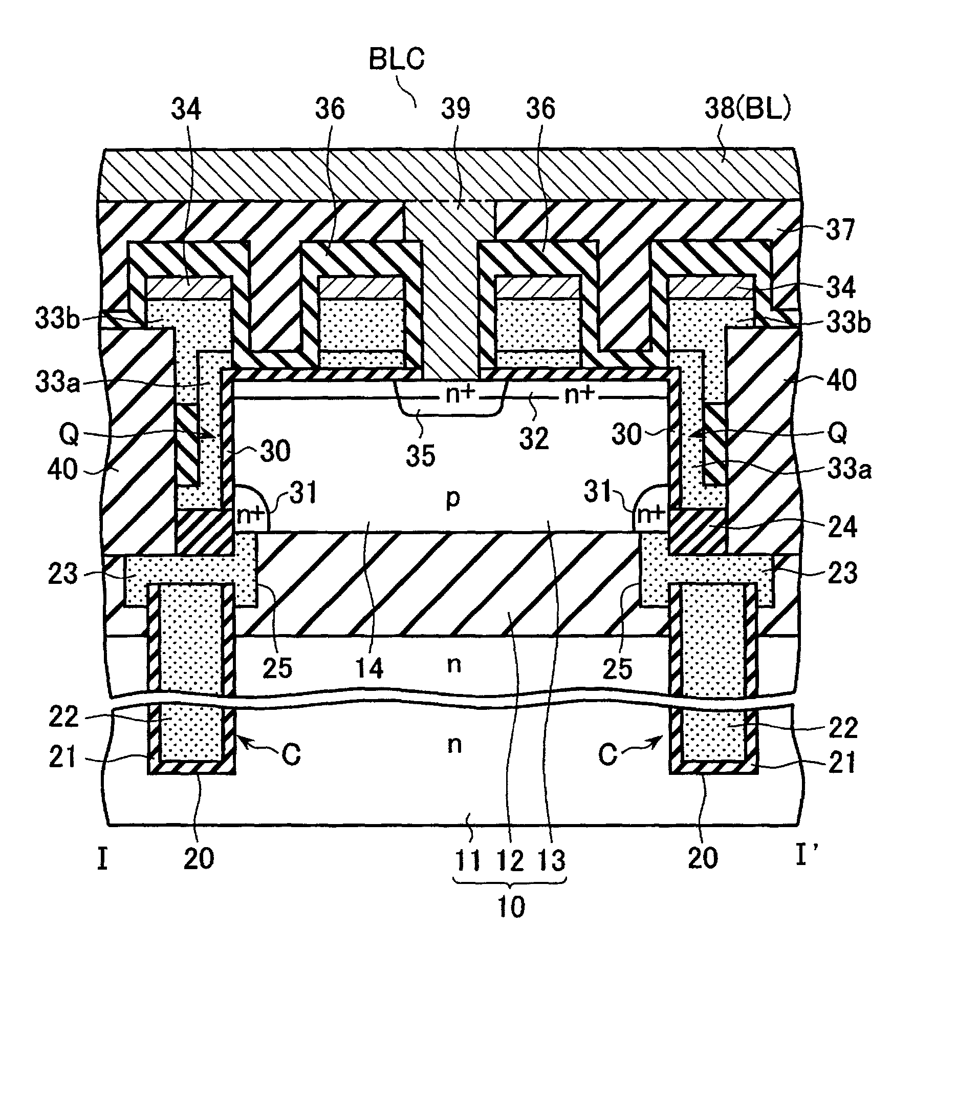
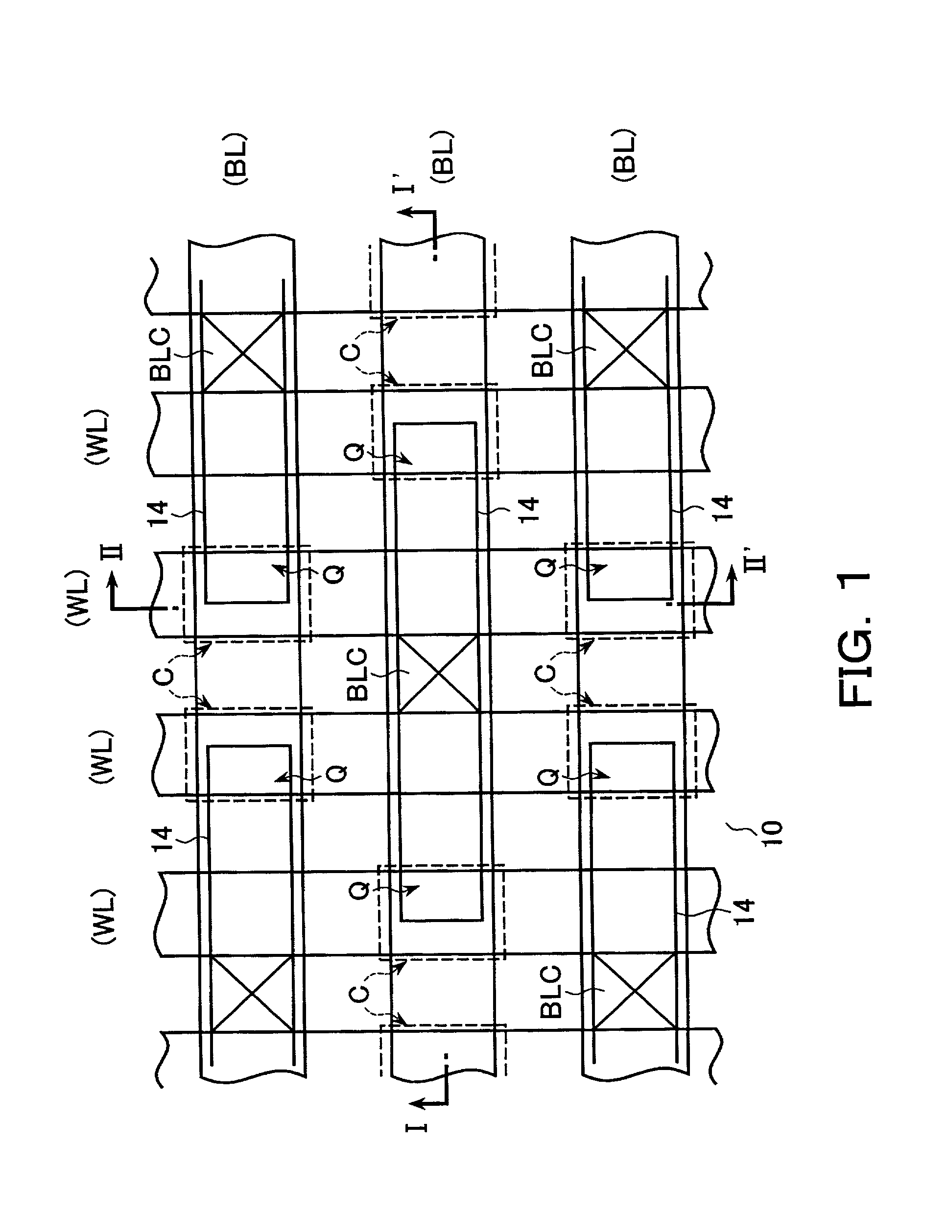
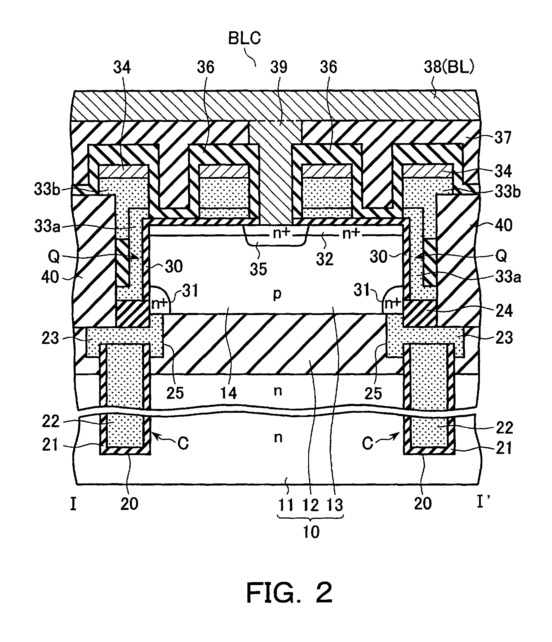
[0038] Referring now to FIG. 1, there is shown a plan view of main part of a trench-capacitor-based dynamic random access memory (DRAM) cell array with half-pitch folded bit line structure in accordance with one embodiment of this invention. Also see FIGS. 2 and 3, which depict cross-sectional views of the structure of FIG. 1 as taken along lines I-I' and II-II' respectively.

[0039] The illustrative embodiment is arranged to employ a silicon-on-insulator (SOI) substrate 10 as an element substrate. This SOI substrate 10 includes a single-crystalline silicon substrate 11 of a selected conductivity type-here, n type. The n-type silicon substrate 11 has its surface on which a silicon oxide film 12 is formed, with a p-type single-crystalline silicon layer 13 formed on the silicon oxide film 12 to thereby make up the multilayer structure of SOI substrate 10. It is necessary that the silicon layer 13 has a predetermined thickness in view of the fact that this layer's thickness...

embodiment 2

[Embodiment 2]

[0058] Turning now to FIG. 10, there is shown a cross-sectional view of a trench DRAM cell array structure in accordance with another embodiment of this invention, in a way corresponding to that of the previously discussed embodiment of FIG. 2. Its plan view is the same as that shown in FIG. 1. A difference of the FIG. 10 embodiment from the above-stated embodiment is that the buried strap 23 is designed to have a two- or "double"-layer structure that consists essentially of n-type polysilicon films 23a, 23b stacked over each other. A first one of these two layers, i.e. polysilicon (poly-Si) film 23a, is fabricated prior to formation of the width-increased groove portion 25 in such a manner such that it is multilayered on a sidewall of the groove 20 at upper part than the storage electrode 22 of capacitor C in the state that no capacitor insulation films are present. And, after having formed the width-increased groove portion 25, the remaining, second-layered poly-Si f...

embodiment 3

[Embodiment 3]

[0070] Referring next to FIG. 18, there is shown a sectional view of a trench DRAM cell array structure in accordance with yet another embodiment of this invention, in a way corresponding to that of the previously stated embodiment of FIG. 2. Its plan view is the same as that shown in FIG. 1. The FIG. 18 embodiment is different from the above-stated embodiment in that i) the width-increased groove portion 25 is formed over the entire thickness range of the silicon oxide film 12, ii) the capacitor C's storage electrode 22 is buried so that its upper surface is located at the width-increased groove portion 25 and thus has an increased area, and iii) its overlying buried strap 23 is so formed as to come into contact with only the bottom surface of p-type silicon layer 13.

[0071] A fabrication process of the FIG. 18 structure will be described with reference to FIGS. 19 to 24. As shown in FIG. 19, after having formed grooves 20 for capacitor use by RIE methods, oxide film e...


PUM


Abstract

A semiconductor device has an element substrate including a semiconductor layer of a first conductivity type being formed over a semiconductor substrate with a dielectric film interposed therebetween. A groove is formed in the element substrate with a depth extending from a top surface of the semiconductor layer into the dielectric film, the groove having a width-increased groove portion in the dielectric film as to expose a bottom surface of the semiconductor layer. An impurity diffusion source is buried in the width-increased groove portion to be contacted with the bottom surface. A transistor is formed to have a first diffusion layer being formed through impurity diffusion from the impurity diffusion source to the bottom surface of the semiconductor layer, a second diffusion layer formed through impurity diffusion to the top surface of the semiconductor layer, and a gate electrode formed at a side face of the groove over the impurity diffusion source with a gate insulation film between the side face and the gate electrode.

Description

[0001] This application is based on and claims the benefit of priority from prior Japanese Patent Application No. 2000-371106, filed on Dec. 6, 2000, the entire contents of which are incorporated herein by reference.[0002] 1. Field of the Invention[0003] This invention relates in general to semiconductor microtechnologies and, in more particular, to highly integrated semiconductor devices with dynamic random access memory (DRAM) cells each having a trench capacitor and a vertical transistor that works perpendicular to the surface of a semiconductor chip. The invention also relates to methodology for fabrication of semiconductor devices of the type stated above.[0004] 2. Description of Related Art[0005] In recent years, DRAM devices employing memory cells each consisting essentially of a single transistor and a single capacitor, also known as "1-transistor / 1-capacitor" cells, are becoming greater in integration or "bit-packing" density virtually endlessly. On-chip areas of such memor...

Claims


Application Information

Patent Timeline
Patent Type & Authority Applications(United States)
IPC IPC(8): H01L21/8242H01L27/108H01L27/12
CPCH01L27/10841H01L27/10864H01L27/1203H01L27/10876H01L27/10891H01L27/10867H10B12/395H10B12/0383H10B12/0385H10B12/053H10B12/488H10B12/00
Inventor YAMADA, TAKASHIKAJIYAMA, TAKESHI
Owner KK TOSHIBA
Why Eureka
Try Eureka