Method for forming Ta2O5 dielectric layer using plasma enhanced atomic layer deposition

Inactive Publication Date: 2002-07-04
INTELLECTUAL DISCOVERY CO LTD
View PDF0 Cites 42 Cited by
  • Summary
  • Abstract
  • Description
  • Claims
  • Application Information

AI Technical Summary

Benefits of technology

0015] A method for forming a Ta.sub.2O.sub.5 dielectric layer using a plasma enhanced atomic lay

Problems solved by technology

Meanwhile, in case of a Ta.sub.2O.sub.5 dielectric layer deposited by the LPCVD (Low Pressure Chemical Vapor Deposition) method, the electric property of a capacitor deteriorates because of inferior step coverage.
First, the poor reactivity of oxygen

Method used


Image

  • Method for forming Ta2O5 dielectric layer using plasma enhanced atomic layer deposition
  • Method for forming Ta2O5 dielectric layer using plasma enhanced atomic layer deposition
  • Method for forming Ta2O5 dielectric layer using plasma enhanced atomic layer deposition

Examples


Embodiment Construction

[0020] The disclosed processes will now be described in conjunction with the accompanying drawings, FIGS. 2A to 2E.

[0021] FIGS. 2A to 2E are cross-sectional views depicting a method for forming Ta.sub.2O.sub.5 dielectric layer in accordance with the disclosed process.

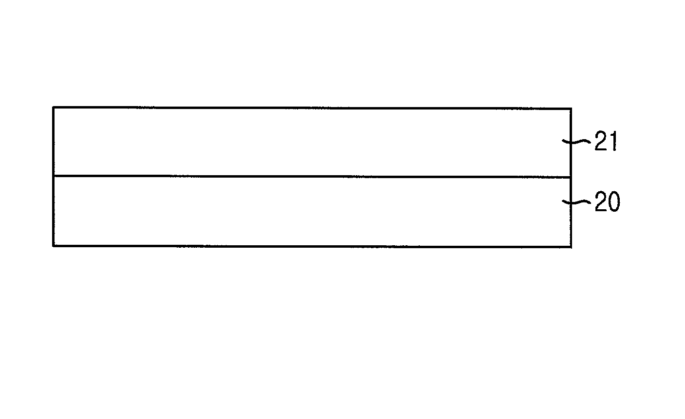
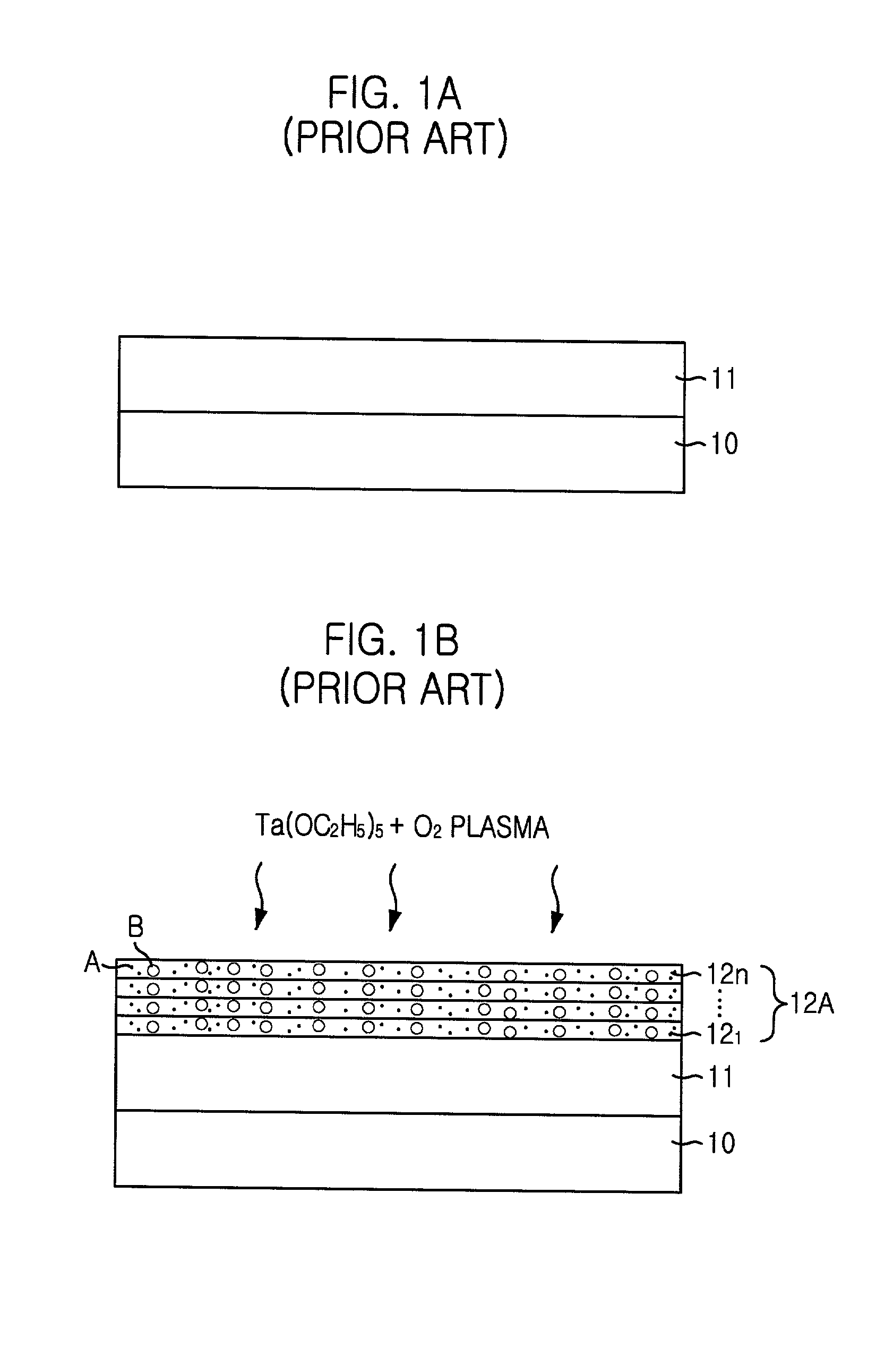
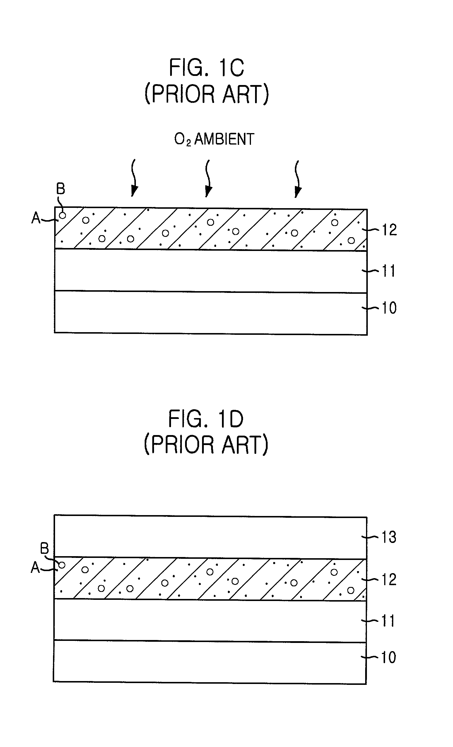
[0022] First, as illustrated in FIG. 2A, after a polysilicon layer 21 to form the bottom electrode is deposited on a substrate 20 formed with the substructure including transistors and plugs, the natural oxidation layer (now shown) on the surface of the polysilicon layer 21 is etched back with HF or BOE (Buffer Oxide Etchant), and then the surface of the polysilicon layer 21 is treated with the RTP (Rapid Thermal Process) in an ambient atmosphere of NH.sub.3.

[0023] Then, as illustrated in FIG. 2B, a Ta.sub.2O.sub.5 dielectric layer 22A is formed by flowing Ta(OC.sub.2H.sub.5).sub.5 source in the chamber and generating Ta and oxygen plasma.

[0024] The method for depositing a Ta.sub.2O.sub.5 dielectric layer 22A using the ...


PUM

PropertyMeasurementUnit
Timeaaaaaaaaaa
Timeaaaaaaaaaa
Pressureaaaaaaaaaa

Abstract

A method for forming a Ta2O5 dielectric layer using plasma enhanced atomic layer deposition, which can improve the quality of a layer and its electric property by forming a Ta2O5 dielectric layer using a plasma enhanced atomic layer deposition. The method for forming a Ta2O5 dielectric layer using plasma enhanced atomic layer deposition, comprising the steps of: a) flowing Ta(OC2H5)5 source gas in a chamber and generating plasma; b) depositing a Ta2O5 layer by using the plasma; c) purging the chamber; d) repeatedly performing the steps a) to c) in order to form a Ta2O5 dielectric layer; e) thermally treating the surface of the Ta2O5 dielectric layer in an oxygen atmosphere; and f) crystallizing the Ta2O5 dielectric layer.

Description

[0001] 1. Technical Field[0002] A method for forming a dielectric layer of a capacitor in a semiconductor device is disclosed. More particularly, a method for forming a Ta.sub.2O.sub.5 dielectric layer using a plasma enhanced atomic layer deposition is disclosed.[0003] 2. Description of the Related Art[0004] As the level of integration increases in semiconductor devices like DRAMs (Dynamic Random Access Memory), superior electrical properties, such as high charge capacity in a limited space and reduced leakage current are needed in a DRAM capacitor. For this reason, a Ta.sub.2O.sub.5 dielectric layer, which is a high dielectric layer, is used for the dielectric layer of the capacitor.[0005] Meanwhile, in case of a Ta.sub.2O.sub.5 dielectric layer deposited by the LPCVD (Low Pressure Chemical Vapor Deposition) method, the electric property of a capacitor deteriorates because of inferior step coverage.[0006] To solve this problem, the atomic layer deposition (ALD) is used to improve t...

Claims


Application Information

Patent Timeline
IPC IPC(8): C23C16/40H01L21/205C23C16/44C23C16/455C23C16/515H01L21/314H01L21/316H01L21/8242H01L27/108
CPCC23C16/405C23C16/45523C23C16/45542C23C16/515C23C16/56H01L21/02183H01L21/02274H01L21/0228H01L21/0234H01L21/02356H01L21/31604
Inventor KIM, KYONG-MINLEE, JONG-MIN
Owner INTELLECTUAL DISCOVERY CO LTD
Why Eureka
Try Eureka