Apparatus for removing native oxide layers from silicon wafers

a technology of silicon wafers and native oxides, applied in biochemistry apparatus and processes, decorative arts, applications, etc., can solve the problems of loss of selectivity and increase the removal rate of native oxides, and achieve the effects of reducing process pressure, improving reaction rate and reducing process costs

Inactive Publication Date: 2002-08-15
STEAG C V D SYTEMS
View PDF0 Cites 10 Cited by
  • Summary
  • Abstract
  • Description
  • Claims
  • Application Information

AI Technical Summary

Benefits of technology

[0011] According to still further features in the described preferred embodiment, the partial pressure of the etchant gas is preferably within the moderate pressure range, of 10-300 Torr. The higher partial pressures would be expected to produce faster reaction rates, but would result in a number of disadvantages. Thus, higher pressures in the reactor increase the danger of leakage of NF.sub.3 from the reactor to the atmosphere, which can cause a serious health problem since NF.sub.3 is highly toxic. In addition, a high pressure in the reactor increases the danger of particles depositing on the silicon wafer being treated which will cause problems in subsequent processing of the wafer. Further, a higher pressure in the reactor increases the wafer processing time in single-wafer processing apparatus, since the NF.sub.3 must be completely removed from the chamber prior to transferring the wafer to the next process module. Thus, a low process pressure saves time by requiring less pump down time at the end of the process, and less time for pressure and flow stabilization at the beginning of the process.

Problems solved by technology

As will be described more particularly below, it has been found that elevating the process temperature as described above substantially increases the removal rate of the native oxide without losing the selectivity achieved at room temperature until the higher end of above-described temperature range is reached At higher temperatures, the native oxide removal rate may increase further, but it was found that selectivity is lost.

Method used


Image

  • Apparatus for removing native oxide layers from silicon wafers
  • Apparatus for removing native oxide layers from silicon wafers
  • Apparatus for removing native oxide layers from silicon wafers

Examples


Embodiment Construction

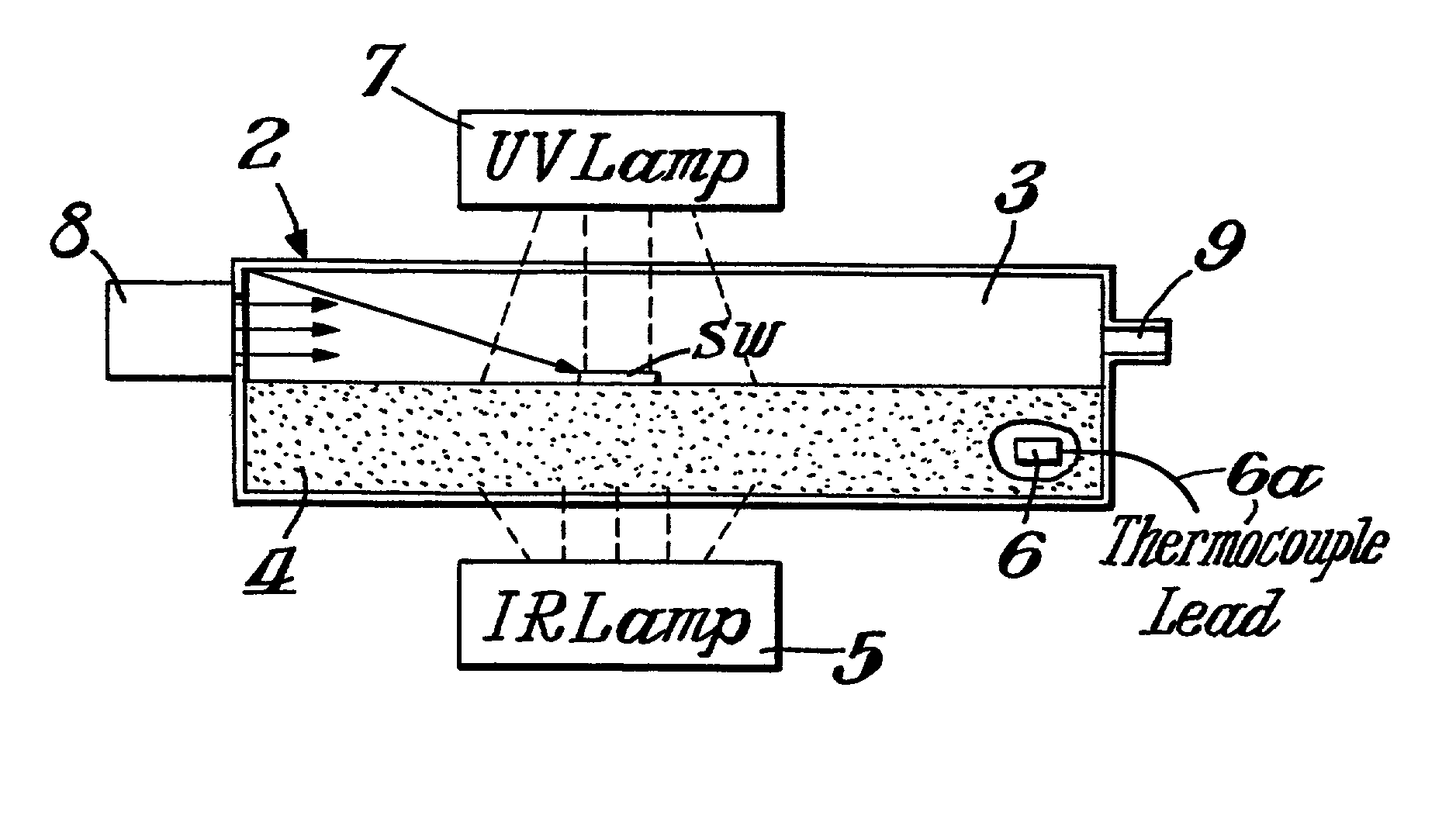
[0019] FIGS. 1 and 2 schematically illustrate one form of apparatus constructed in accordance with the present invention for cleaning silicon wafers by selectively removing a native oxide layer from the silicon wafer without significantly affecting the underlying silicon, or a polysilicon or thermal oxide deposition that may be thereon.

[0020] The apparatus illustrated in FIGS. 1 and 2 includes a reactor, generally designated 2, consisting of a horizontal quartz tube defining an internal reactor chamber 3. The horizontal quartz tube may be about 85 mm in length, about 15 mm in diameter, and about 2 mm wall thickness. The lower half of reactor chamber 3 is occupied by a half-cylinder shaped graphite susceptor 4 which supports one of more silicon wafers SW to be processed within the reactor chamber. Externally of and below reactor chamber 3 is an infrared lamp 5 which heats the graphite susceptor 4 from below. The graphite susceptor has a thermo-couple 6 embedded within it for temperat...


PUM

PropertyMeasurementUnit
temperatureaaaaaaaaaa

Abstract

A method and apparatus for selectively removing a native oxide layer from a silicon wafer without significantly affecting the underlying silicon or other material, that may be thereon, by exposing the silicon wafer to an etchant gas including NF3 while simultaneously exposing the wafer to ultraviolet radiation, and heating the wafer to a temperature of 100-400° C.

Description

[0001] This application is related to Provisional Application No. 60 / 086,635, filed May 20, 1998 and claims its priority date.FIELD AND BACKGROUND OF THE INVENTION[0002] The present invention relates to a method and apparatus for selectively removing native oxide layers from silicon wafers without significantly affecting the underlying silicon, or without significantly removing other materials, such as polysilicon or thermal oxide depositions, that may be thereon. Such a process is of substantial importance to the semiconductor industry since the selective removal of native oxide from silicon wafers is among the most frequently performed processes in fabricating silicon semiconductor devices.[0003] Whenever a silicon wafer is exposed to an oxidizing environment, a native oxide layer tends to form on the silicon wafer. Such native oxide layers would deleteriously affect the subsequent processing steps performed on the silicon wafer, and therefore must be cleanly and quickly removed w...

Claims


Application Information

Patent Timeline
Patent Type & Authority Applications(United States)
IPC IPC(8): B08B7/00C12N15/867H01L21/306H01L21/311
CPCB08B7/0057H01L21/02046H01L21/31116
Inventor NEMIROVSKY, YAELSTOLYAROVA, SARABROSILOW, BENJAMIN
Owner STEAG C V D SYTEMS
Why Eureka
Try Eureka