
Active matrix liquid crystal display device and switching element used therein

a liquid crystal display device and active matrix technology, applied in the direction of identification means, instruments, optics, etc., can solve the problems of pixel potential, uneven display, and reduced luminance of a modul

Inactive Publication Date: 2002-08-22
NEC LCD TECH CORP
View PDF0 Cites 9 Cited by
  • Summary
  • Abstract
  • Description
  • Claims
  • Application Information

AI Technical Summary

Benefits of technology

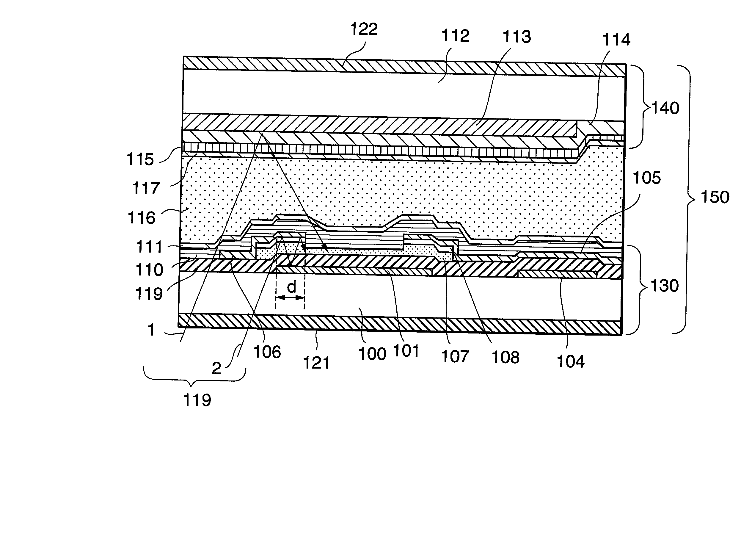
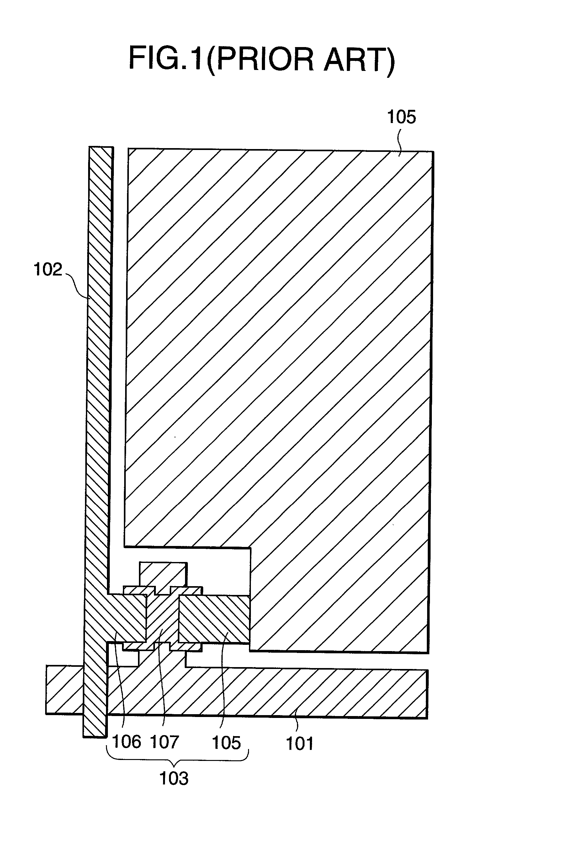
[0049] FIG. 7 shows a TFT having a structure that oblique light from the backlight located opposite to the liquid crystal 116 enters the TFT substrate 130 and is reflected entering the front channel portion easily. In this case, the drain electrode 106 or the source (pixel) electrode 105 of the TFT is formed so that the width thereof becomes wider than that of the amorphous silicon film 107, in other words, so that the area that the amorphous silicon film does not exist under the electrode in the channel width direction exists corresponding to the area of the drain electrode 106 or the source (pixel) electrode 105 extending over the amorphous silicon film in the channel width direction. Therefore, light entering the crosshatched area having a relatively low optical absorption (due to no optical absorption by the amorphous silicon film) obliquely from underneath with respect to the gate line 101 is reflected at the electrode and easily reaches the channel portion.
[0054] Then, using the drain electrode 106 and the source (pixel) electrode 105 as an etching mask, the n.sup.+ amorphous silicon film 108 on the amorphous silicon film 107 is removed to avoid short-circuiting of the drain electrode 106 and the source (pixel) electrode 105 on the amorphous silicon film 107, thereby completing the formation of the TFT 103. Thereafter, a second insulating film 110 is formed to cover and protect the TFT 103, the drain line 102 and the source (pixel) electrode 105, and the TFT substrate 130 is completed. An alignment film made of an organic material for aligning the liquid crystal 116 is coated on the second insulating film 110 followed by alignment processing, thus forming a first alignment film 111.
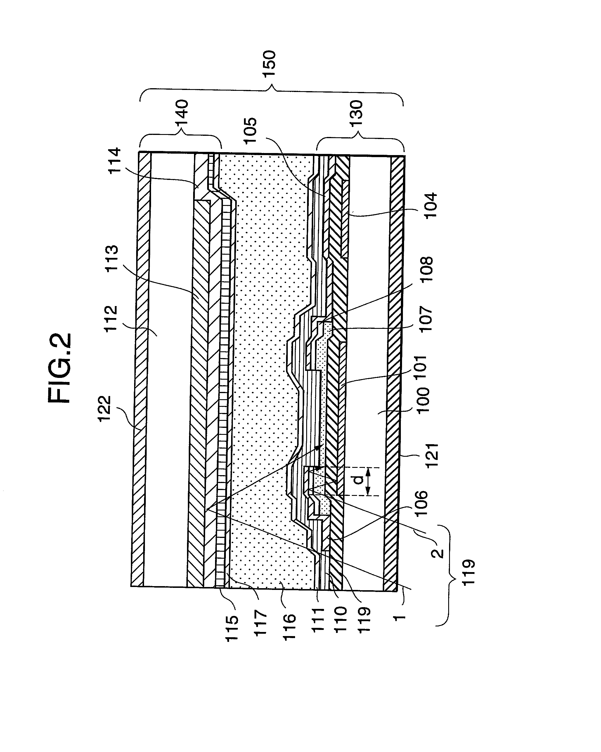
[0059] The active matrix liquid crystal display device according to the first embodiment operates in a manner similar to that of the conventional active matrix liquid crystal display device as follows: first, a signal from the liquid crystal drive circuit 152 is inputted to the liquid crystal display panel 150; and the TFT 103 disposed in each segment in a matrix form is turned on; and then, an electric field is generated between the source (pixel) electrode 105 and the common electrode 104; and thereafter, the liquid crystal 116 sealed between both substrates 140 and 130 brings about an electro optic effect, changing the light transmittance of the liquid crystal display panel 150; and as a result, light 119 emitted from the backlight 151 undergoes transmittance modulation via the liquid crystal display panel 150 as shown in FIG. 6, so that the light intensity changes pixel by pixel, thereby enabling image display on the device.
[0096] By reducing the light-induced OFF leak current as a result of the intensity of light incident on the channel portion of the TFT 103, being lowered through the above-described means, the reduction of flickering and the improvement of display uniformity can be realized.SECOND EMBODIMENT
[0101] The electric operation of the active matrix liquid crystal display device according to the second embodiment is similar to that of the active matrix liquid crystal display device according to the first embodiment. However, the second embodiment is different from the first embodiment as follows: different from the first embodiment, the amorphous silicon film 107 is entirely included in the gate line 101 as shown in the cross-sectional view of FIG. 17 and therefore, light from the backlight passing through the end portion of the gate line 101 toward inside of the device reflects multiple times between the gate line 101 and the drain electrode 106 or between the gate line 101 and the source (pixel) electrode 105 before traveling the distance, "optimal overlap length `d`," which is determined by a source or drain electrode overlapping a gate electrode in a channel length direction; and as a result, the attenuation of the incident light becomes more noticeable than that achieved by the active matrix liquid crystal display device according to the first embodiment, thereby ensuring greater reduction in flickering and better display uniformity. Conclusively, the optimal overlap length "d" having the same value as that of the first embodiment is sufficient in the second embodiment.

Problems solved by technology

The light-induced OFF leak current lowers the pixel potential, thus resulting in various undesirable shortcomings, such as reduced luminance of a module, uneven display and flickering.
In case of TFTs which are used in a liquid crystal display panel for a monitor, an on-board display or the like, the backlight luminance is increased to meet the demand for high luminance display, the light-induced OFF leak current generated in the semiconductor region by incident light cannot be solved by the existing techniques alone.
The above-described conventional methods for reducing light-induced OFF leak current are insufficient to suppress the light-induced OFF leak current and further suppression of light-induced OFF leak current needs to be carried out.
However, in the case where a low-reflectance resin which is often used in an active matrix liquid crystal display device driven in a lateral electric field mode or the like is used as a light shielding film on the opposing substrate, since the very amount of the light reflected by the light shielding film reduces because of the low reflectance of the light shielding film, the effect in reducing light-induced OFF leak current becomes relatively smaller, in other words, does not influence seriously even when the above-described two schemes are employed in the device.

Method used


Image

  • Active matrix liquid crystal display device and switching element used therein
  • Active matrix liquid crystal display device and switching element used therein
  • Active matrix liquid crystal display device and switching element used therein

Examples


first embodiment

[0045] the invention will be explained with reference to the accompanying drawings.

[0046] FIG. 4 is a plan view of a unit pixel of a thin-film-transistor array substrate 130 of an active matrix liquid crystal display device according to the first embodiment, and shows the portion of the device figured on the lower side of the cross-sectional view of FIG. 6. FIG. 5 is an enlarged plan view of a thin film transistor portion of each unit pixel. FIG. 6 is a cross-sectional view taken along A-A' in FIG. 4, also illustrating the portion of the device opposite to the thin-film-transistor array substrate 130.

[0047] As shown in FIGS. 4 through 6, the active matrix liquid crystal display device according to the first embodiment of the invention has a overall construction comprising a thin-film-transistor array substrate (hereinafter referred to as TFT substrate) 130, a transparent opposing substrate 140 provided apart from and in parallel to the TFT substrate 130, and a liquid crystal 116 int...

second embodiment

[0097] The second embodiment of the invention will be explained with reference to the accompanying drawings.

[0098] FIG. 15 is a plan view of a unit pixel of a TFT substrate 130 of an active matrix liquid crystal display device according to the second embodiment, and shows the portion of the device figured on the lower side of the cross-sectional view of FIG. 6. FIG. 16 is an enlarged plan view of a thin film transistor portion of each unit pixel. FIG. 17 is a cross-sectional view taken along B-B' in FIG. 15, also illustrating the portion of the device opposite to the TFT substrate 130.

[0099] The active matrix liquid crystal display device according to the second embodiment illustrated in FIG. 15 is different from the active matrix liquid crystal display device according to the first embodiment illustrated in FIGS. 4 to 6 in the points that the amorphous silicon film 107 is entirely included in the gate line 101. That is, the elements constituting the TFT 103 are formed so as to sati...


PUM

PropertyMeasurementUnit
refractive indexaaaaaaaaaa
channel lengthaaaaaaaaaa
outgoing angle θ0aaaaaaaaaa

Abstract

A thin film transistor is designed in such a manner that a semiconductor region includes source and drain electrodes in a channel width direction and further, a planar source-side overlap area constructed by a gate electrode, the source electrode and the semiconductor region and a planar drain-side overlap area constructed by the gate electrode, the drain electrode and the semiconductor region exist. An optimal overlap length of one of the source-side and drain-side overlap areas in a channel length direction is determined, for instance, to be 4 mum, for a light incident on a channel portion of the thin film transistor to have a light intensity below or equal to 0.2% of a light intensity of the backlight incident toward the thin film transistor, thereby reducing a light-induced OFF leak current sufficiently and further improving flickering and display uniformity.

Description

[0001] 1. Field of the Invention[0002] The present invention relates to an active matrix liquid crystal display device and a switching element used therein, and, more particularly, to an active matrix liquid crystal display device having an excellent display uniformity in addition to low level flickering and a switching element used in the display device.[0003] 2. Description of the Prior Art[0004] Thin film transistors (TFTs) are widely used as switching elements in drive circuits for various devices. The use of TFTs in active matrix liquid crystal display devices is particularly remarkable. In case where the semiconductor region of a TFT is formed of amorphous silicon, which is often used in a liquid crystal display or the like, incident light from a backlight or a light source for display generates photocarriers in the semiconductor region. As the photocarriers travel in a channel portion, a light-induced OFF leak current is produced. The light-induced OFF leak current lowers the...

Claims


Application Information

Patent Timeline
Patent Type & Authority Applications(United States)
IPC IPC(8): G02F1/1335G02F1/13357G02F1/1333G02F1/1343G02F1/136G02F1/1368G09F9/00G09F9/30G09F9/35H01L21/336H01L29/786
CPCG02F1/1368G02F1/136
Inventor SHIGA, SHUNSUKETAMURA, FUMINORIKUROHA, SHOUICHIWATANABE, MAKOTO
Owner NEC LCD TECH CORP
Learn More