Thin film transistor and active matrix type liquid crystal display device

Inactive Publication Date: 2002-08-29
HITACHI LTD
View PDF4 Cites 53 Cited by
  • Summary
  • Abstract
  • Description
  • Claims
  • Application Information

AI Technical Summary

Problems solved by technology

For this reason, since the back light is employed in order to light up the display screen, the power consumption becomes large.
Thus, if during the display operation of the liquid crystal display device, Vth is increas

Method used


Image

  • Thin film transistor and active matrix type liquid crystal display device
  • Thin film transistor and active matrix type liquid crystal display device
  • Thin film transistor and active matrix type liquid crystal display device

Examples


Embodiment Construction

[0045] An embodiment of the present invention will hereinbelow be described in detail with reference to the accompanying drawings.

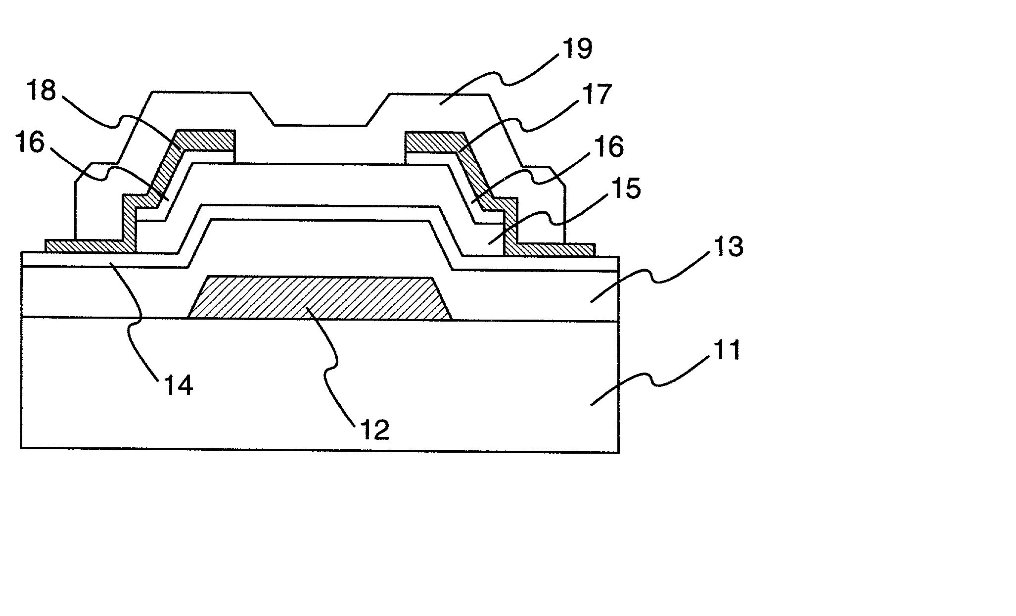
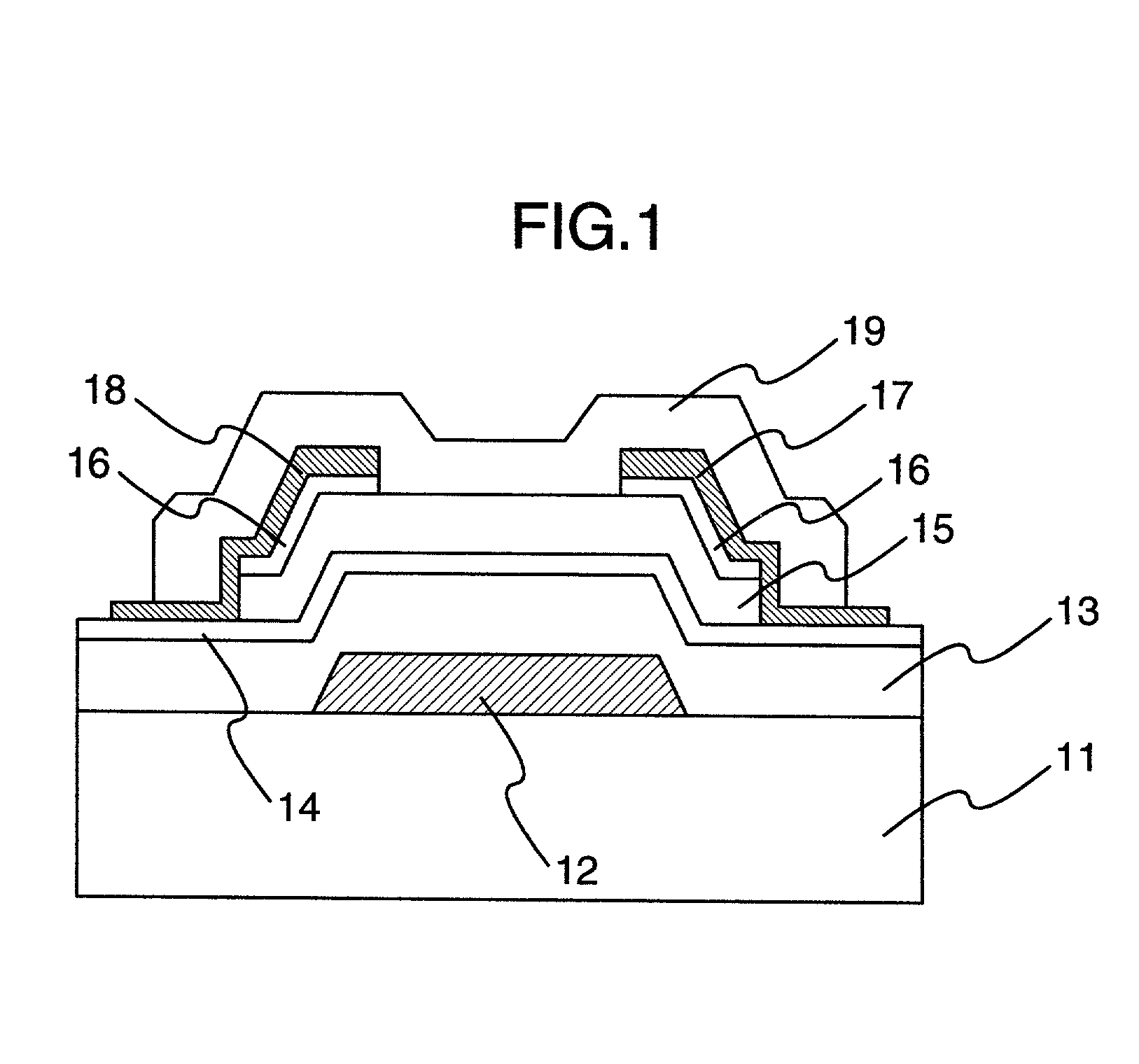
[0046] FIG. 1 is a vertical cross sectional view of a thin film transistor according to an embodiment of the present invention. In FIG. 1, a thin film transistor in the present embodiment is formed into the so-called inverted stagger structure in which a source electrode and a drain electrode are fabricated above a gate electrode, and the elements of the thin film transistor are fabricated on a glass substrate 11. That is, a gate electrode 12 made of Cr, a first insulating layer (gate insulating film) 13 made of silicon nitride, a second gate insulating layer (gate insulating film) 14 made of silicon oxide, a semiconductor layer 15 made of amorphous silicon, a contact layer 16 made of n.sup.+ type amorphous silicon doped with phosphorus, a source electrode 17 and a drain electrode 18 each of which is made of Cr, and a passivation insulating layer (passiva...


PUM


Abstract

A gate electrode, a gate insulating layer, a semiconductor layer, a drain electrode, a source electrode and a passivation insulating layer are fabricated in turn on an insulating substrate, thereby forming a thin film transistor. The thin film transistor is designed in such a way that a silicon oxide film is employed as a second gate insulating layer adjacent to the semiconductor layer; a thickness of the silicon oxide film is set to the range of 0.5 to 3.0 nm; and it shows the characteristics in which when a stress voltage which is negative with respect to the drain electrode and the source electrode is applied to the gate electrode, the operating threshold voltage is reduced.

Description

[0001] 1. Field of the invention[0002] The present invention relates in general to a thin film transistor and an active matrix type liquid crystal display device. More particularly, the invention relates to a thin film transistor which is suitable for being employed as a switching device showing the enhancement type switching characteristics, and an active matrix type liquid crystal display device employing the same.[0003] 2. Description of the Related Art[0004] In general, in active matrix type liquid crystal display devices, a large number of thin film transistors are adopted as the switching devices in display units and drive units. The thin film transistor shows the so-called switching operation in which as the gate voltage is increased with a fixed voltage applied to a drain electrode and a source electrode, at the time when the gate voltage becomes equal to or larger than a predetermined value, the value of a current which is caused to flow through the drain and source is abru...

Claims


Application Information

Patent Timeline
IPC IPC(8): G02F1/1368G09F9/30H01L21/336H01L29/49H01L29/786
CPCH01L29/4908H01L29/78669
Inventor ANDO, MASAHIKOKAWASAKI, MASAHIROWAKAGI, MASATOSHI
Owner HITACHI LTD
Why Eureka
Try Eureka