Semiconductor device, circuit board, electro-optical device, and electronic apparatus

a technology of semiconductor devices and circuit boards, applied in semiconductor devices, optics, instruments, etc., can solve the problems of carrier concentration being liable to increase, degradation over time arising, performance deterioration, etc., and achieve the effect of reducing the degradation of semiconductor films, reducing the degradation of circuits over time, and efficient release of heat generated in semiconductor films

Inactive Publication Date: 2002-09-12
138 EAST LCD ADVANCEMENTS LTD
View PDF3 Cites 9 Cited by
  • Summary
  • Abstract
  • Description
  • Claims
  • Application Information

AI Technical Summary

Benefits of technology

0015] A sixth semiconductor device of the present invention comprises a semiconductor film, a gate insulating film formed on at least part of the semiconductor film, and a gate electrode formed on the gate insulating film. Ends of the semiconductor film comprise regions formed of an intrinsic semiconductor which is not doped with dopant. The regions formed of an intrinsic semiconductor at the ends of the semiconductor film of the semiconductor device less contribute to the transfer of carriers. Even if a high electric field strength or high carrier concentration is generated in the regions formed of an intrinsic semiconductor, therefore, degradation in performance over time can be reduced. In this specification, "a region formed of an intrinsic semiconductor which is not doped with dopant" means a semiconductor region which is doped with a smaller amount of dopant than the other semiconductor regions as well as a region which does not doped with any dopant.
0016] A seventh semiconductor device of the present invention comprises a semiconductor film, a gate insulating film formed on at least part of the semiconductor film, and a gate electrode formed on the gate insulating film. The semiconductor film comprises a region formed of an intrinsic semiconductor which is not doped with dopant and the region extends past the gate electrode. This semiconductor device has a structure in which deterioration caused by heating the semiconductor film when the device is driven or when electric power is applied to the device can be prevented. If the semiconductor device is used as a semiconductor device which is incorporated into, for example, shift registers, level shifters, buffer circuits, and analog switches, degradation of these circuits over time can be reduced.
0017] An eighth semiconductor device of the present invention comprises a semiconductor film having a source region and a drain region, a gate insulating film formed on at least part of the semiconductor film, and a gate electrode formed on the gate insulating film. The semiconductor film comprises a region formed of an intrinsic semiconductor which is not doped with dopant, the region extending toward the source region or the drain region from the gate electrode. As examples of this semiconductor device, thin-film transistors shown in FIGS. 7 and 8 are cited. These thin-film transistors have a structure in which heat generated in the semiconductor film can be efficiently released. If the thin-film transistors are used as a semiconductor device which is incorporated into circuits, such as shift registers, level shifters, buffer circuits, and analog switches, degradation of these circuits over time can be reduced.

Problems solved by technology

Heretofore, semiconductor devices such as MOS elements have had a problem in that their performance deteriorates over time while the devices are operated for a long time.
The degradation over time arising from this cause is significant in some semiconductor devices, such as thin-film transistors, which include a thin semiconductor film serving as an active layer on the insulating layer.
In addition, since the thickness of the semiconductor film is small, the carrier concentration is liable to increase.

Method used


Image

  • Semiconductor device, circuit board, electro-optical device, and electronic apparatus
  • Semiconductor device, circuit board, electro-optical device, and electronic apparatus
  • Semiconductor device, circuit board, electro-optical device, and electronic apparatus

Examples


first embodiment

[0059] (First Embodiment)

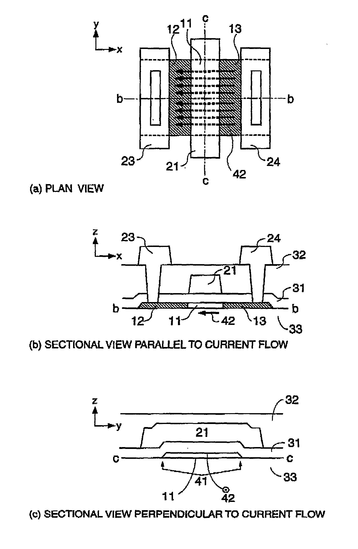
[0060] FIG. 4 is composed of a schematic plan view and two sectional views of a thin-film transistor according to a first embodiment of the present invention. In the thin-film transistor, a semiconductor film composed of a highly-doped source region 12, a highly-doped drain region 13, and an active region 11 is formed of polycrystalline silicon. The thin-film transistor, basically, has the same structure as the conventional, typical thin-film transistor shown in FIG. 1. However, as shown in FIG. 4, a gate electrode 21 is disposed so as not to cover ends of the semiconductor film composed of the highly-doped source region 12, the highly-doped drain region 13, and the active region 11. Also, a sub gate electrode 22 connected with the gate electrode 21 is formed so as to extend past ends 41 of the semiconductor film.

[0061] The distributions of the electric field strength and the carrier concentration of the thin-film transistor according to this embodiment were...

second embodiment

[0064] (Second Embodiment)

[0065] FIG. 6 is composed of a schematic plan view and two sectional views of a thin-film transistor according to a second embodiment of the present invention. In the thin-film transistor, a semiconductor film composed of the highly-doped source region 12, the highly-doped drain region 13, and the active region 11 has an intrinsic-semiconductor region 14 at ends thereof. Since the intrinsic-semiconductor region 14 is not in the flow of current 42, deterioration in the performance of the device over time, which is due to a high electric field strength and a high carrier concentration, can be reduced even if the high electric field strength and the high carrier concentration occur in the intrinsic-semiconductor region 14.

third embodiment

[0066] (Third Embodiment)

[0067] FIG. 7 is a schematic plan view of a thin-film transistor according to a third embodiment of the present invention and FIG. 8 is a sectional view of the thin-film transistor in the direction perpendicular to the current flow. A sectional view in the direction parallel to current flow is substantially the same as shown in FIG. 6(b) and is thus omitted. The semiconductor film of the thin-film transistor shown in FIG. 7 is separated into a plurality of portions by a plurality of intrinsic-semiconductor regions 14 disposed in parallel with a current 42 flowing between the source and the drain. This structure is suitable to reduce degradation over time caused due to a high electric field strength and a high carrier concentration which occur at the end potions of the semiconductor film, thus releasing heat generated while the current flows. In addition, since the intrinsic-semiconductor region 14 is formed simply by doping a desired position or area with do...


PUM

PropertyMeasurementUnit
widthaaaaaaaaaa
semiconductoraaaaaaaaaa
electric poweraaaaaaaaaa

Abstract

The width of a gate electrode is smaller than that of the semiconductor film. A sub gate electrode connected to the gate electrode is disposed, at the gate electrode side of the semiconductor film, away from the semiconductor film more than gate electrode. The width of the sub gate electrodes is larger than that of the semiconductor film. Ends of the semiconductor film have regions formed of an intrinsic semiconductor which is not doped with dopant. In a semiconductor device, this structure is suitable to reduce degradation over time which is due to increase of the electric field strength or the carrier concentration at the ends of the semiconductor film.

Description

[0001] The present invention relates to semiconductor devices, and more particularly to a semiconductor device, an electro-optical device, and an electronic apparatus in which degradation in performance over time can be prevented.[0002] FIG. 1 shows a thin-film transistor as an example of a conventional semiconductor device. FIG. 1(a) is a plan view of a conventional polycrystalline-silicon thin-film transistor, FIG. 1(b) is a sectional view taken along the line b-b in the plan view, and FIG. 1(c) is a sectional view taken along the line c-c in the plan view. As shown in FIG. 1, the polycrystalline-silicon thin-film transistor generally has a top gate structure (Liquid Crystal Display Technology written and edited by Shoichi Matsumoto, published by Sangyo Tosho).[0003] FIG. 2 shows a manufacturing process of a typical polycrystalline-silicon thin-film transistor. First, an amorphous silicon layer is formed on a glass substrate 51 by PECVD using SiH.sub.4 or LPCVD using Si.sub.2H.sub...

Claims


Application Information

Patent Timeline
Patent Type & Authority Applications(United States)
IPC IPC(8): G02F1/1368H01L27/12H01L29/423H01L29/786
CPCG02F1/1368H01L27/12H01L29/42384H01L29/78609H01L29/786
Inventor KIMURA, MUTSUMI
Owner 138 EAST LCD ADVANCEMENTS LTD
Why Eureka
Try Eureka